Electron Devices and Circuits: Unit I: PN Junction Devices
Full Wave Rectifier
Circuit Diagram, Operations, Calculation, Formula, Advantages, Solved Example Problem
• The full wave rectifier conducts during both positive and negative half cycles of input a.c. supply. In order to rectify both the half cycles of a.c. input, two diodes are used in this circuit.
Full Wave Rectifier
AU
: Dec.-O9, 10, 11, 13, May-15, 17
•
The full wave rectifier conducts during both positive and negative half cycles
of input a.c. supply. In order to rectify both the half cycles of a.c. input,
two diodes are used in this circuit. The diodes feed a common load RL
with the help of a centre tap transformer. The a.c. voltage is applied through
a suitable power transformer with proper turns ratio.
•
The full wave rectifier circuit is shown in the Fig. 1.16.1.

•
For the proper operation of the circuit, a centre-tap on the secondary winding
of the transformer is essential.
1. Operation of the Circuit
•
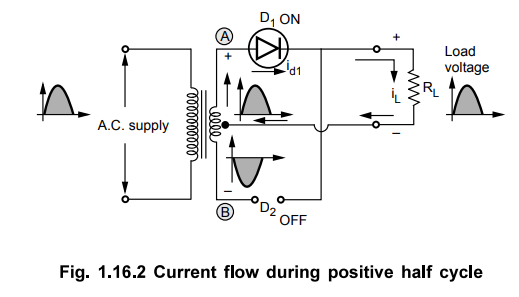
Consider the positive half cycle of a.c. input voltage in which terminal (A) is
positive and terminal (B) negative. The diode D1 will be forward biased and
hence will conduct; while diode D2 will be reverse biased and will act as an
open circuit and will not conduct. This is illustrated in the Fig. 1.16.2.
•
The diode D1 supplies the load current, i.e. iL = idl. This current
is flowing through upper half of secondary winding while the lower half of
secondary winding of the transformer carries no current since diode D2
is reverse biased and acts as an open circuit.
•
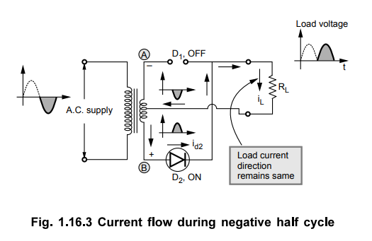
In the next half cycle of a.c. voltage, polarity reverses and terminal (A)
becomes negative and (B) positive. The diode D2 conducts, being
forward biased, while D1 does not, being reverse biased. This is
shown in the Fig. 1.16.3.
•
The diode D2 supplies the load current, i.e. iL = id2 .
Now the lower half of the secondary winding carries the current but the upper
half does not.
•
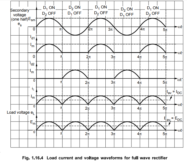
It is noted that the load current flows in both the half cycles of a.c. voltage
and in the same direction through the load resistance. Hence we get rectified
output across the load. The load current is sum of individual diode currents
flowing in corresponding half cycles. It is also noted that the two diodes do
not conduct simultaneously but in alternate half cycles. The individual diode
currents and the load current are shown in the Fig. 1.16.4.
•
Thus the full wave rectifier circuit essentially consists of two half wave
rectifier circuits working independently (working in alternate half cycles of
a.c.) of each other but feeding a common load. The output load current is still
pulsating d.c. and not pure d.c.
2. Maximum Load Current
•
Let Rf = Forward resistance of diodes, Rs = Winding
resistance of each half of secondary
•
RL = Load resistance, eg = Instantaneous a.c. voltage
across each half of secondary
em
= Esm sin ωt where ω = 2πf
Esm
= Maximum value of a.c. input voltage across each half of secondary winding.
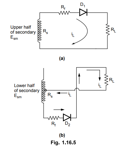
•
Hence we can write the expression for the maximum value of the load current,
looking at equivalent circuit shown in the Fig 1.16.5.
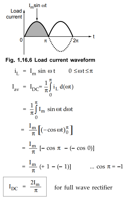
3. Average D.C. Load Current (lDC)
•
Consider one cycle of the load current iL from 0 to - to obtain the average
value which is d.c. value of load current.
•
For half wave it is I /n and full wave rectifier is the combination of two half
wave circuits acting alternately in two half cycles of input. Hence obviously
the d.c. value for full wave circuit is 2 Im/π
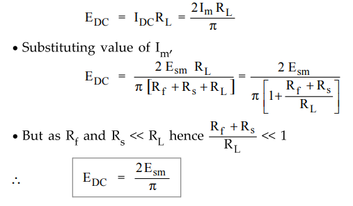
4. Average D.C. Load Voltage (EDC)
•
The d.c. load voltage is,
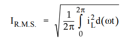
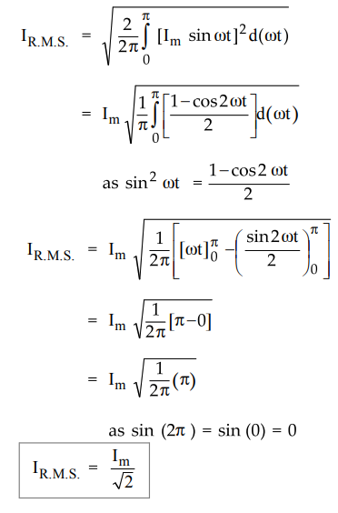
5. RMS Load Current (IRMS)
•
The R.M.S. value of current can be obtained as follows :
•
Since two half wave rectifier are similar in operation we can write,
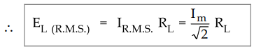
6. R.M.S. Value of the Load Voltage
As
the load is resistive, the r.m.s. value of the load voltage is given by,
7. D.C. Power Output (PDC)
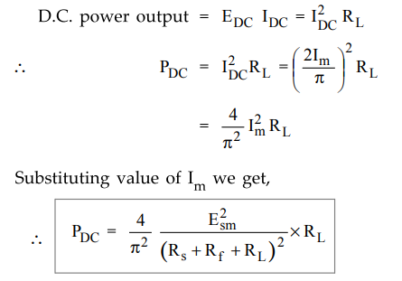
Key
Point : Instead of remembering this formula,
students can use the expression EDCIDC or I2DCRL
to calculate PDC while solving the problems.
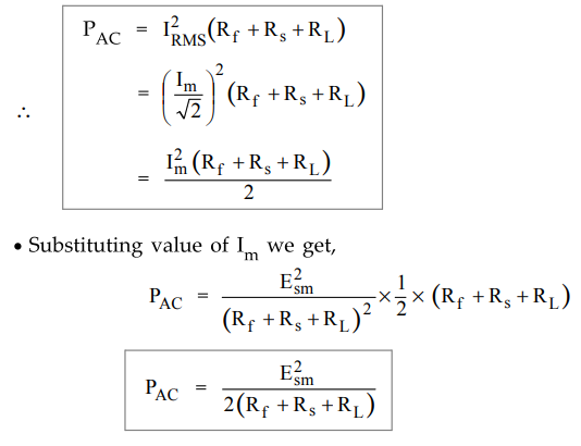
8. A.C. Power Input (PAC)
•
The a.c. power input is given by,
9. Rectifier Efficiency (η)

10. Ripple Factor (ɤ)
•
As derived earlier in case of half wave rectifier the ripple factor is given by
a general expression,
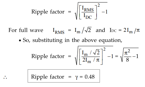
Key
Point : This indicates that the ripple contents in the
output are 48 % of the d.c. component which is much less than that for the half
wave circuit.
11. Load Current (IL)
•
The Fourier for the load current is obtained by taking the sum of the series
for the individual rectifier current. The two diodes conduct in alternate half
cycles, i.e. there is a phase difference of π radians between two diode
currents, Hence,
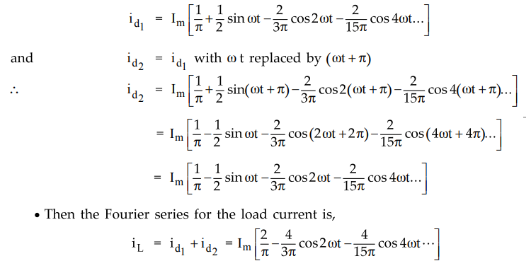
•
The first term in the above series represents the average or d.c. value, while
the remaining terms "ripple". It is seen that the lowest frequency of
the ripple is 2f, i.e. twice the supply frequency of a.c. supply. The lowest
ripple frequency in the load current of the full-wave connection, is double
than that in the half-wave connection.
•
As seen from the Fig. 1.16.2 and Fig. 1.16.3 the individual diode currents are
flowing in opposite directions through the two halves of the secondary winding.
Hence the net secondary current will be difference of individual diode
currents.
Thus, isec = id1 - id2
•
The Fourier series of isec is obtained by the difference between the
series of individual diode currents. Using above relations we can write,
isec
= Im sin ω t
•
Hence under ideal conditions, the secondary current is purely sinusoidal. No
d.c. component flows through the secondary hence there is no danger of
saturation. This reduces the transformer losses and overall size and cost of
the circuit. Thus the transformer gets utilised effectively.
12. Peak Inverse Voltage (PIV)
•
It can be observed from the circuit diagram that when the diode is reversed
biased then full transformer secondary voltage gets impressed across it. The
drop across conducting diode is assumed zero. Thus the peak value of the
inverse voltage to which diode gets subjected is voltage across both the parts
of the transformer secondary. This is shown in the Fig. 1.16.7.
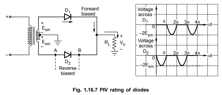
•
It can be seen that when D2 is reverse biased, point A is at – Esm
with respect to ground while point B is at + Esm with respect to ground,
neglecting diode drop. Thus total peak voltage across D2 is 2Esm
PIV
of diode = 2 Esm = π EDC|IDC = 0
•
where Esm = Maximum value of a.c. voltage across half the secondary of
transformer. If the diode drop is considered to be 0.7 V then the PIV of
reverse biased diode is,
PIV
of diode = 2Esm - 0.7
This
is because only one diode conducts at a time.
13. Transformer Utilization Factor (T.U.F.)
•
In full wave rectifier, the secondary current flows through each half
separately in every half cycle. While the primary of transformer carries
current continuously. Hence T.U.F. is calculated for primary and secondary
windings separately and then the average T.U.F. is determined.
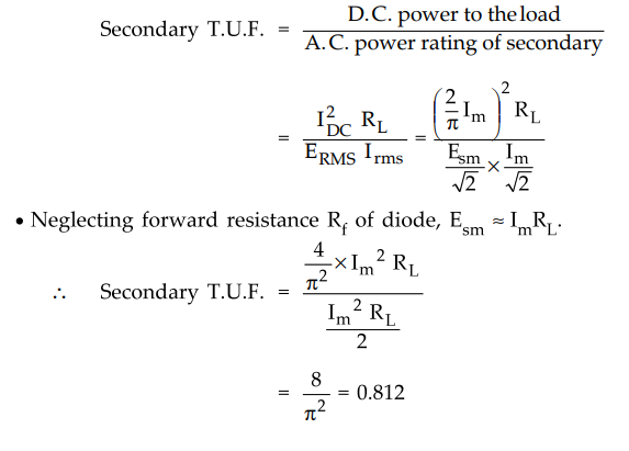
The
primary of the transformer is feeding two half-wave rectifiers separately.
These two half-wave rectifiers work independently of each other but feed a
common load. We have already derived the T.U.F. for half wave circuit to be
equal to 0.287. Hence,
T.U.F.
for primary winding = 2 × T.U.F. of half wave circuit
=
2 × 0.287 = 0.574
The
average T.U.F for fullwave circuit will be
AVerageT
. U . F . for full wave rectifier circuit = T . U . F . of primary + T . U . F . of secondary
/ 2
0.574
+ 0.812 / 2 = 0.693
Average
T.U.F. for full-wave rectifier = 0.693
Key
Point: Thus in full wave circuit transformer gets
utilized more than the half wave rectifier circuit.
14. Voltage Regulation
For
a full wave circuit,
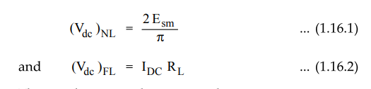
The
regulation can be expressed as,
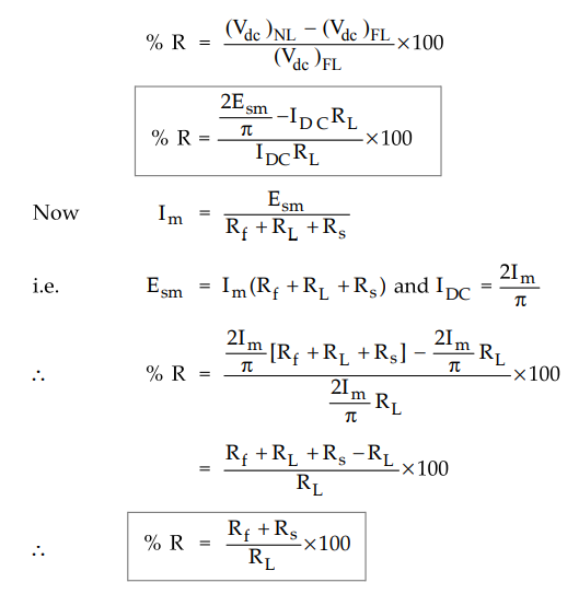
•
Neglecting winding resistance Rs, the regulation can be expressed as,
%
R ≈ Rf / RL × 100
where
Rf = Forward resistance of the diode.
•
The regulation characteristics is drooping, as discussed earlier in case of
half wave rectifier as output voltage decreases as load increases from no load
to full load.
15. Advantages of Full Wave Rectifier
1.
The d.c. load voltage and current are more than half wave.
2.
No d.c. current through transformer windings hence no possibility of
saturation.
3.
T.U.F. is better as transformer losses are less.
4.
The efficiency is higher.
5.
The large d.c. power output.
6.
The ripple factor is less.
16. Disadvantages of Full Wave Rectifier
1.
The PIV rating of diode is higher.
2.
Higher PIV diodes are larger in size and costlier.
3.
The cost of centre tap transformer is higher.
17. comparison of Full Wave and Half Wave Circuit
•
For comparison, we assume that the full-wave and half-wave circuits use
identical diodes, identical load resistances and the voltage across half the
secondary winding of transformer used in full-wave circuit is the same as the
voltage across the secondary winding of the transformer used in half-wave
circuit.
1.
The d.c. load current in case of full wave circuit is twice to that in half
wave circuit; similarly the d.c. load voltage in full wave circuit is twice
that in half wave circuit.
2.
The lowest ripple frequency in full wave circuit is twice that in half wave
circuit. Now to remove ripple, the additional circuits called filter circuits
are used along with rectifier circuits. But as the frequency is more in
full-wave, the capacitor values required in capacitance filter are much less
hence smaller elements are sufficient in filter circuits used with full wave
circuit to reduce ripple.
3.
Because there is no net d.c. current through windings of the transformer used
in full wave circuit, the losses are less as compared to losses in transformer
used in half wave circuit.
4.
The full wave connection gives d.c. power output four times as large, when
compared with half wave connection.
5.
The efficiency of rectification in a full wave connection is twice that for
half wave connection.
6.
The ripple factor is less for full-wave, i.e. rectification is more nearly
complete for full wave as compared to half-wave.
Ex.
1.16.1 If the required D.C. output voltage is 9 V, assuming ideal diodes,
calculate the A.C. r.m.s. input voltage required in the following cases :
i)
Half wave rectifier, ii) Centre-tapped full wave rectifier.
Sol.
:
EDC = 9 V, Ideal diodes
i)
Half wave rectifier :
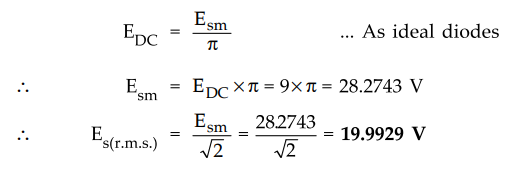
•
This is required a.c. r.m.s. input voltage on secondary of transformer.
ii)
Centre-tapped full wave rectifier :
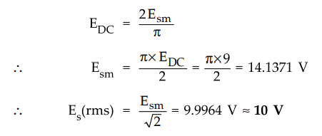
•
This is required a.c. r.m.s voltage on input side from either end of secondary
to center tap.
•
Thus the transformer secondary rating must be 10 V - 0 - 10 V.
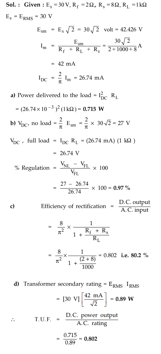
Ex.
1.16.2 A full-wave rectifier circuit is fed from a transformer having a
centre-tapped secondary winding. The rms voltage from either and of secondary
to center tap is 30 V. If the diode forward resistance is 2 Ω and that of the
half secondary is 8 Ω, for a load of 1 k Ω,
calculate, a) Power delivered to load , b) % Regulation at full load, c)
Efficiency of recitification, d) T..U.F. of secondary.
Sol
: Given
Review Questions
1. Explain the operation of FWR with centre tap transformer with
neat circuit diagram. Also derive the following for this rectifier : i) dc
output voltage ii) dc output current iii) RMS output voltage iv) Ripple factor
v) Peak inverse voltage
AU : Dec.-09,10,ll, Marks 16; Dec.-13, Marks 8
2. Derive the expressions for the following parameters of the
full wave rectifier.
a) Average d.c. current (IDC)
b) Average d.c. output voltage (EDC)
c) R.M.S. value of current (IRMS)
d) D.C. power output (PDC)
e) A.C. power input (PAC)
f) Rectifier efficiency (η).
3. Prove that the ripple factor for the full-wave rectifier
circuit is 0.48.
4. Compare the full wave rectifier with half-wave rectifier
circuit.
5. Derive the expression for maximum efficiency of a full wave
rectifier.
6. A full-wave rectifier circuit is fed from a transformer
having a centre-tapped secondary winding. The r.m.s. voltage from either end of
secondary to center tap is 20 V. If the diode forward resistance is 3 Ω and that
of the half secondary is 5 Ω, for a load of 1 hΩ, calculate
a) Power delivered to load, b) % Regulation at full load, c)
Efficiency at full load, d) T.U.F. of secondary.
(Ans.: a) Pdc = 0.3191 W, b) % Regulation = 0.7469 %,
c) Efficiency of full load = 0.8041, d) T.U.F. = 0.804)
7. Explain the action of a full-wave rectifier using diodes and
give waveforms of input and output voltages.
AU : May-15, Marks 8
Electron Devices and Circuits: Unit I: PN Junction Devices : Tag: : Circuit Diagram, Operations, Calculation, Formula, Advantages, Solved Example Problem - Full Wave Rectifier
Related Topics
Related Subjects

Electron Devices and Circuits
EC3301 3rd Semester EEE Dept | 2021 Regulation | 3rd Semester EEE Dept 2021 Regulation