Linear Integrated Circuits: Unit IV: Special ICs
565 PLL Applications
with Block Diagram, Operating working principle
1. Frequency Multiplier 2. Frequency Synthesizer 3. FM Demodulator 4. Frequency Shift Keying (FSK) Demodulator 5. AM Detection 6. Frequency Translation
565 PLL Applications
May-03,04,05,07,08,09,11,12,15,17,18,
Dec.-03,04,05,06,07,08,09,10,11,16
1. Frequency Multiplier
Fig.
4.5.1 shows the block diagram for a frequency multiplier using PLL 565. Here, a
divide by N network is inserted between the VCO output (pin 4) and the phase
comparator input (pin 5). Since the output of the divider is locked to the
input frequency fir the VCO is actually running at a multiple of the input
frequency.
Therefore,
in the locked state, the VCO output frequency fo is given by,
fo
= Nf i... (4.5.1)

By
selecting proper divider by N network, we can obtain desired multiplication.
For example, to obtain output frequency lo= 6 I'j, a divide by N should be
equal to 6.
Fig.
4.5.2 shows LM 565 IC used as a frequency multiplier circuit. The IC 7490 is a
4 bit binary counter. It is configured as a divide by 10 circuit.

2. Frequency Synthesizer
The
PLL can be used as the basis for frequency synthesizer that can produce a
precise series of frequencies that are derived from a stable crystal controlled
oscillator. Fig. 4.5.3 shows the block diagram of frequency synthesizer. It is
similar to frequency multiplier circuit except that divided by M network is
added at the input of phase lock loop. The frequency of the crystal-controlled
oscillator is divided by an integer factor M by divider network to produce a
frequency fosc/M, where fosc is the frequency of the crystal controlled
oscillator. The VCO frequency fVCO is similarly divided by factor N
by divider network to give frequency equal to fvco/N. When the PLL is locked in
on the divided-down oscillator frequency, we will have fosc /M = fVCO
/N, so that fVCO = (N/M) fosc.

By
adjusting divider counts to desired values large number of frequencies can be
produced, all derived from the crystal controlled oscillator.
3. FM Demodulator
The
PLL can be very easily used as an FM detector or demodulator. Fig. 4.5.4 shows
the block diagram of FM detector.

When the PLL is locked in on the FM signal, the VCO frequency follows the instantaneous frequency of the FM signal, and the error voltage or VCO control voltage is proportional to the deviation of the input frequency from the centre frequency. Therefore, the a-c component of error voltage or control voltage of VCO will represent a true replica of the modulating voltage that is applied to the FM carrier at the transmitter. The faithful reproduction of modulating voltage depends on the linearity between the instantaneous frequency deviation and the control voltage of VCO. It is also important to note that the FM frequency deviation and the modulating frequency should remain in the locking range of PLL to get the faithful replica of the modulating signal. If the product of the modulation frequency fm and the frequency deviation exceeds the (ΔfC)2, the VCO will not be able to follow the instantaneous frequency variations of the FM signal.
4. Frequency Shift Keying (FSK) Demodulator
In
digital data communication, binary data is transmitted by means of a carrier
frequency. It uses two different carrier frequencies for logic 1 and logic 0
states of binary data signal. This type of data transmission is called
Frequency Shift Keying (FSK). In this data transmission, on the receiving end,
two carrier frequencies are converted into 1 and 0 to get the original binary
data. This process is called FSK demodulation.
A
PLL can be used as a FSK demodulator, as shown in the Fig. 4.5.5. It is similar
to the PLL demodulator for analog FM signals except for the addition of a
comparator to produce a reconstructed digital output signal.
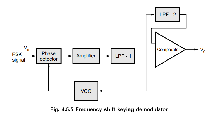
Let
us consider that there are two frequencies, one frequency (f1) is
represented as "0" and other frequency (f2) is represented
as "1". If the PLL remain is locked into the FSK signal at both f 1
and f 2, the VCO control voltage which is also supplied to the
comparator will be given as
VC1
= (f1 - fo ) / Kv
VC2
= (f2 - fo ) / Kv, respectively.
where
Kv is the voltage to frequency transfer coefficient of the VCO.
The
difference between the two control voltage levels will be ΔVC = (f2
– f1 ) / Kv The reference voltage for the comparator is
derived from the additional low pass filter and it is adjusted midway between VC1
and VC2 . Therefore, for VC1 and VC2,
comparator gives output '0' and '1', respectively.
5. AM Detection
A
PLL can be used to demodulate AM signals as shown in Fig. 4.5.6.

The
PLL is locked to the carrier frequency of the incoming AM signal. Once locked
the output frequency of VCO is same as the carrier frequency, but it is in
unmodulated form.
The
modulated signal with 90° phase shift and the unmodulated carrier from output
of PLL are fed to the multiplier. Since VCO output is always 90° out of phase
with the incoming AM signal under the locked condition, both the signals
applied to the multiplier are in same phase. Therefore, the output of the
multiplier contains both the sum and the difference signals. The low pass
filter connected at the output of the multiplier rejects high frequency
components gives demodulated output. As PLL follows the input frequencies with
high accuracy, a PLL AM detector exhibits a high degree of selectivity and
noise immunity which is not possible with conventional peak detector type AM
modulators.
6. Frequency Translation
The
frequency translation means shifting the frequency of an oscillator by a small
factor. Fig. 4.5.7 shows the block schematic for frequency translator using
PLL.

It
consists of mixer, low pass filter and the PLL. The input frequency fs
which has to be shifted is applied to the mixer. Another input to the mixer is
the output voltage of VCO, fo. Therefore, the output of mixer
contains the sum and difference signal (fo ± fs). The low
pass filter connected at the output of mixer rejects the (fo + fs)
signal and gives only (f0 - l's) signal at the output. The (f0- fs) signal is
applied to the phase detector. Another input for phase detector is the offset
frequency f1. In the locked mode, the VCO output frequency is
adjusted to make two input frequencies of phase detector equal. This gives
fo
- fs = f1 and
fo
= fs + f1
By
adjusting offset frequency f1 we can shift the frequency of the
oscillator to the desired value.
Review Questions
1. Explain AM
demodulation using PLL.
2. Discuss the
application of PLL as frequency synthesizer.
3. Explain the
applications of PLL as frequency translator and FM demodulator.
May-08, 12, Dec.-12,
Marks 8
4. Narrate the process
of FSK demodulation using PLL.
5. What is PLL ?
Explain its application as a frequency multiplier.
Dec.-ll, 12, 16, May-15,
Marks 8
6. How frequency
multiplication is done in PLL ?
7. Briefly explain the
functional block diagram of NE 565 PLL-IC to operate as a frequency divider.
Linear Integrated Circuits: Unit IV: Special ICs : Tag: : with Block Diagram, Operating working principle - 565 PLL Applications
Related Topics
Related Subjects

Linear Integrated Circuits
EE3402 Lic Operational Amplifiers 4th Semester EEE Dept | 2021 Regulation | 4th Semester EEE Dept 2021 Regulation