Electron Devices and Circuits: Unit IV: Multistage and Differential Amplifiers
A.C. Analysis of Differential Amplifier using h-Parameters
• In the a.c. analysis, we will calculate the differential gain Ad, common mode gain Ac, input resistance Ri and the output resistance Ro of the differential amplifier circuit, using the h-parameters.
A.C. Analysis of Differential Amplifier using h-Parameters
AU
: Dec.-l0, 14, 15, 16, May-13, 14, 15
•
In the a.c. analysis, we will calculate the differential gain Ad, common mode
gain Ac, input resistance Ri and the output resistance Ro of the differential
amplifier circuit, using the h-parameters.
1. Differential Gain (Ad)
•
For the differential gain calculation, the two input signals must be different
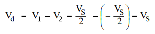
from each other. Let the two a.c. input signals be equal in magnitude but
having 180° phase difference in between them. The magnitude of each a.c. input
voltage VS1 and VS2 be VS/2
•
The two a.c. emitter currents Ie1 and Ie2 are equal in
magnitude and 180° out of phase. Hence they cancel each other to get resultant
a.c. current through the emitter as zero. Hence for the a.c. purposes emitter
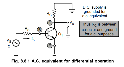
terminal can be grounded. The a.c. small signal differential amplifier circuit
with grounded emitter terminal is shown in the Fig. 8.8.1. As the two
transistors are matched, the a.c. equivalent circuit for the other transistor
is identical to the one shown in the Fig. 8.8.1.
•
Thus the circuit can be analysed by considering only one transistor. This is
called as half circuit concept of analysis.
•
The approximate hybrid model for thee above circuit can be shown as in the Fig.
8.8.2, neglecting hoe,
•
Applying KVL to the input loop,
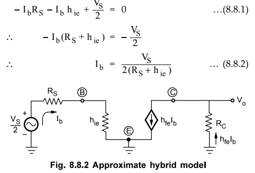
Applying
KVL to the input loop,
Vo
= -hfe Ib RC … (8.8.3)
Substituting
equation (8.8.2) in equation (8.8.3)
The
negative sign indicates the phase difference between input ad output.
Now
two input signal magnitudes are -2 but they are opposite in polarity, as 180°
out of phase.
The magnitude of the differential gain Ad is
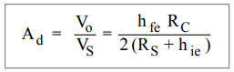
(For imbalanced output) ... (8.8.5)
Where
VS = Differential input
Key
Point: The differential gain obtained in the equation
(8.7.5) is for the circuit where output is measured with respect to ground. So
it is unbalanced output.
•
We are interested to obtain A, for the differential amplifier with the balanced
output. Balanced output is across the two collectors of the transistors Q1 and
Q2, which are perfectly matched. Such balanced output is double than that
obtained above, with unbalanced output. Hence the expression for Ad with
balanced output changes as
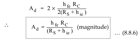
•
This is the differential gain for balanced output dual input differential
amplifier circuit.
2. Common Mode Gain (Ac)
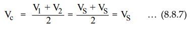
•
Let the magnitude of both the a.c. input signals be Vs and are in phase with
each other. Hence the differential input V1 = 0 while the common mode input V
is the average value of the two.
•
While the output can be expressed as,
Vo
= Ac VS ... (8.8.8)
Ac
= Vo / Vs … (8.8.8a)
•
But now both the emitter currents Ie1 = Ie2 = Ie,
flows through RE in the same direction.
•
Hence the total current flowing through RE is 2 Ie.
•
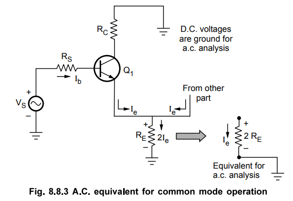
As the two transistors are matched, a.c. equivalent of common mode operation
can be shown, considering only one transistor, as in the Fig. 8.8.3.
•
The approximate hybrid model for the above circuit can be shown as in the Fig.
8.8.4.

•
As the current through RE is 2Ie, for simplicity of derivation the current can
be assumed to be Ie and effective emitter resistance as 2 RE. Hence the emitter
resistance is shown 2 RE in the Fig. 8.8.4.
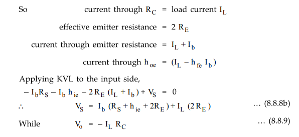
Negative
sign due to the assumed direction of current. Applying KVL to the output loop,
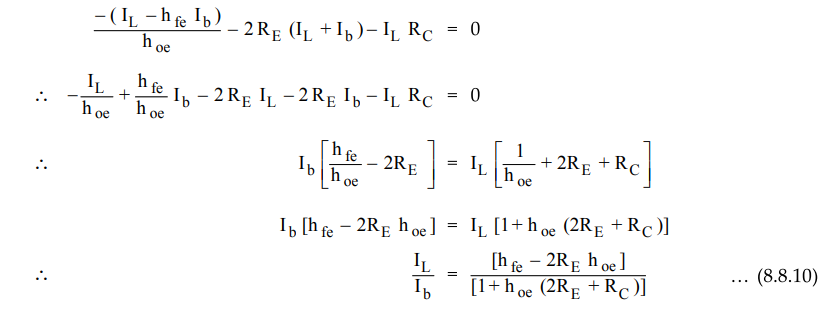
Substituting
value of Ibz into the equation (8.8.8b), we get
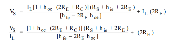
Finding
L.C.M. and adjusting the terms, we get
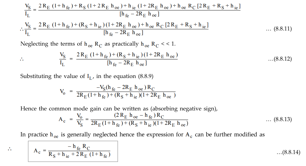
Key
Point: The expression for Ac remains same whether the
output is balanced or unbalanced.
3. Common Mode Rejection Ratio (CMRR)
•
Once the differential and common mode gains are obtained, the expression for
the CMRR can be obtained as,
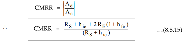
•
This is CMRR for dual input balanced output differential amplifier circuit.
4. Differential Input Impedance (Ri)
•
It is the equivalent resistance between one of the input and the ground when
the other input terminal is grounded. Hence
Ri
= Vs / Ib
•
But referring to Fig. 8.8.2 and equation (8.8.1) we can write,
Ri
= 2 (RS + hie )
•
For one transistor and input pair, the input resistance is Rg+hie hence for
dual input circuit the total input resistance is 2 (RS + hie ),
as the two circuits are perfectly matched.
Key
Point : This input resistance is not dependent on
whether output is balanced or unbalanced.
5. Output Impedance
•
It is defined as the equivalent resistance between one of the output terminals
with respect to ground. As seen from the Fig. 8.8.2, the resistance between
output terminal with respect to ground is RC.
Ro
= RC …. (8.8.18)
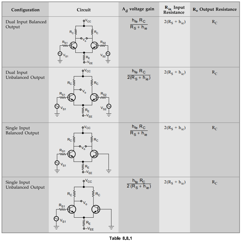
•
In the a.c. analysis of dual input, balanced output differential amplifier, it
can be observed that the results are derived by considering only one transistor
and one output at the time of analysis. And then due to matched pair of
transistors, the results are derived for dual input, balanced output
configuration. Hence the results for the remaining configurations can be
directly obtained from the results derived earlier. And hence the summary of
the differential amplifier circuit configurations is directly provided in the
Table 8.8.1.
Ex.
8.8.1 The Fig. 8.8.5 shows dual input, balanced output differential amplifier
configuration. Assuming silicon transistors with hie = 2.8 kii calculate i)
Operating point values ii) Differential gain iii) Common mode gain iv) CMRR
v)
Output if Vsi = 70 mV peak to peak at 1 kHz and VS2 = 40 mV peak to
peak at 1 kHz.

Sol.
:
As the transistors are silicon,
VBE
= 0.7 V
i)
Operating point values are ICQ and VCEQ
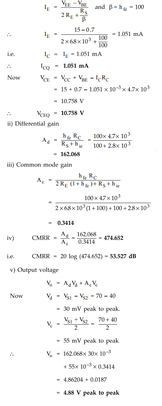
Key
Point : In practice AcVc can be
neglected as compared to AdVd as common mode gain is
always very small compared to differential gain.
Review Question
1. Draw the circuit diagram of an emitter, coupled BJT
differential amplifier and derive expressions for differential gain, common
mode gain, CMRR, input impedance and output impedance.
AU
: Dec.-10, 14, 15, 16, May-13, 14, 15, Marks 16
Electron Devices and Circuits: Unit IV: Multistage and Differential Amplifiers : Tag: : - A.C. Analysis of Differential Amplifier using h-Parameters
Related Topics
Related Subjects

Electron Devices and Circuits
EC3301 3rd Semester EEE Dept | 2021 Regulation | 3rd Semester EEE Dept 2021 Regulation