Linear Integrated Circuits: Unit II: Characteristics of Op-amp
A.C. Analysis of Differential Amplifier using h-Parameters
Working Principle, Mode Operation, Circuit Diagram, Solved Example Problems | Op-amp
In the a.c. analysis, we will calculate the differential gain Ad, common mode gain Ac, input resistance Ri and the output resistance R0 of the differential amplifier circuit, using the h-parameters.
A.C. Analysis of Differential Amplifier using h-Parameters
In
the a.c. analysis, we will calculate the differential gain Ad,
common mode gain Ac, input resistance Ri and the output
resistance R0 of the differential amplifier circuit, using the h-parameters.
1. Differential Gain(Ad)
For
the differential gain calculation, the two input signals must be different from
each other. Let the two a.c. input signals be equal in magnitude but having
180° phase difference in between them. The magnitude of each a.c. input voltage
VS1 and VS2 be VS/2
The
two a.c. emitter currents Ie1 and Ie2 are equal in
magnitude and 180° out of phase. Hence they cancel each other to get resultant
a.c. current through the emitter as zero. This is already discussed in the
section 2.8.1. Hence for the a.c. purposes emitter terminal can be grounded.
The a.c. small signal differential amplifier circuit with grounded emitter
terminal is shown in the Fig. 2.8.1. As the two transistors are matched, the
a.c. equivalent circuit for the other transistor is identical to the one shown
in the Fig. 2.8.1.
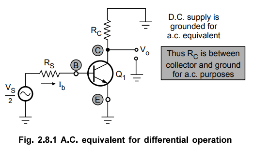
Thus
the circuit can be analysed by considering only one transistor. This is called
as half circuit concept of analysis.
The
approximate hybrid model for the above circuit can be shown as in the Fig.
2.8.2, neglecting hoe,
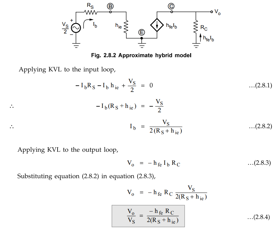
The
negative sign indicates the phase difference between input and output.
Now
two input signal magnitudes are VS/2 but they are opposite in
polarity, as 180o out of phase.
Vd = V1 – V2
= VS / 2 – (-VS/2) = VS|
The
magnitude of the differential gain Ad is
Where
VS = Differential input
Key
Point The differential gain obtained in the equation
(2.8.5) is for the circuit where output is measured with respect to ground. So
it is unbalanced output.
We
are interested to obtain Ad for the differential amplifier with the balanced
output. Balanced output is across the two collectors of the transistors Q1
and Q2, which are perfectly matched. Such balanced output is double
than that obtained above, with imbalanced output. Hence the expression for Ad
with balanced output changes as
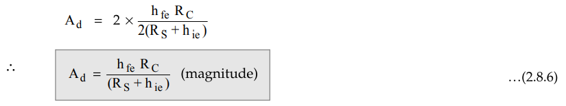
This
is the differential gain for balanced output dual input differential amplifier
circuit.
2. Common Mode Gain(Ac)
Let
the magnitude of both the a.c. input signals be VS and are in phase
with each other. Hence the differential input Vd = 0 while the
common mode input VC is the average value of the two.
Vc
= V1 + V2 / 2 = VS + VS / 2 ….
(2.8.7)
While
the output can be expressed as
Vo
= Ac VS …. (2.8.8)
Ac
= Vo / VS ….
(2.8.8 (a))
But
now both the emitter currents Ie1 = Ie2 = Ie,
flows through RE in the same direction.
Hence
the total current flowing through RE is 2 Ie.
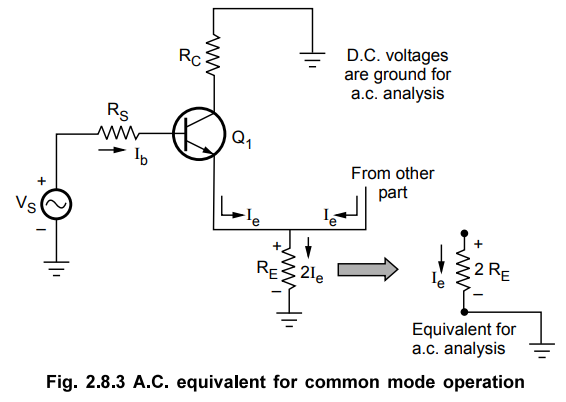
As
the two transistors are matched, a.c. equivalent of common mode operation can
be shown, considering only one transistor, as in the Fig. 2.8.3.
The
approximate hybrid model for the above circuit can be shown as in the Fig.
2.8.4.
As
the current through RE is 2Ie, for simplicity of
derivation the current can be assumed to be Ie and effective emitter resistance
as 2 RE. Hence the emitter resistance is shown 2 RE in
the Fig. 2.8.4.
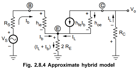
So Current through RC = Load
current IL
Effective
emitter resistance = 2 RE
Current
through emitter resistance = IL + Ib
Current
through hoe = (IL - hfe Ib)
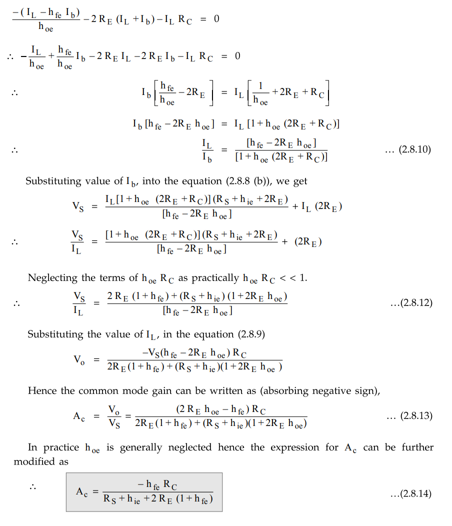
Applying
KVL to the input side,
Negative
sign due to the assumed direction of current. Applying KVL to the output loop,
Key
Point The
expression for Ac remains same whether the output is balanced or
unbalanced.
3. Common Mode Rejection Ratio (CMRR)
Once
the differential and common mode gains are obtained, the expression for the
CMRR can be obtained as,
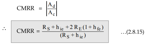
This
is CMRR for dual input balanced output differential amplifier circuit.
4. Differential Input Impedance (Ri)
It
is the equivalent resistance between one of the input and the ground when the
other input terminal is grounded. Hence
Ri
= VS / Ib …. (2.8.16)
But
referring to Fig. 2.8.2 and equation (2.8.1) we can write,
Ri
= 2 (RS + hie) ….
(2.8.17)
For
one transistor and input pair, the input resistance is RS +hie hence for dual
input circuit the total input resistance is 2(RS + hie),
as the two circuits are perfectly matched.
Key
Point This input resistance is not dependent on
whether output is balanced or unbalanced.
5. Output Impendance (Ro)
It
is defined as the equivalent resistance between one of the output terminals
with respect to ground. As seen from the Fig. 2.8.2, the resistance between
output terminal with respect to ground is RC.
Ro
= RC …. (2.8.18)
In
the a.c. analysis of dual input, balanced output differential amplifier, it can
be observed that the results are derived by considering only one transistor and
one output at the time of analysis. And then due to matched pair of
transistors, the results are derived for dual input, balanced output
configuration. Hence the results for the remaining configurations can be
directly obtained from the results derived earlier. And hence the summary of
the differential amplifier circuit configurations is directly provided in the
Table 2.8.1.

Example
2.8.1 The Fig. 2.8.5 shows dual input, balanced output differential amplifier
configuration. Assuming silicon transistors with hie = 2.8 AΩ
calculate
i)
Operating point values
ii)
Differential gain
iii)
Common mode gain
iv)
CMRR
v)
Output if VS1 = 70 mV peak to peak at 1 kHz and VS2 = 40
mV peak to peak at 1 kHz.
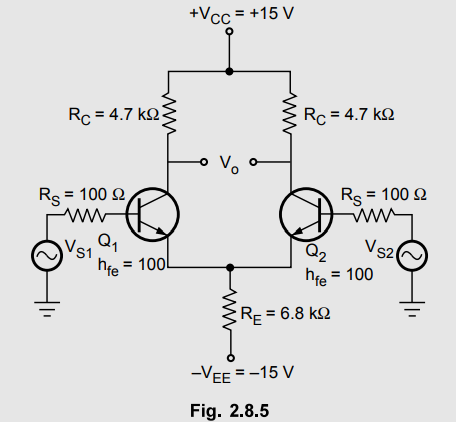
Solution
:
As the transistors are silicon,
VBE = 0.7 V
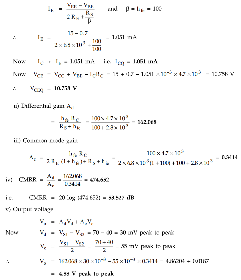
i)
Operating point are ICQ and VCEQ
Key
Point In practice AcVc can be
neglected as com pared to AffVd «s common mode gain is always very small
compared to differential gain.
6. Differential Amplifier with Constant Current Source
Without
physically increasing the value of RE, the RE is replaced by a
transistor operated at a constant current.
Such
a constant currrent source circuit gives the effect of a very high resistance
without affecting the Q point values of the differential amplifier.
The
differential amplifier using constant current bias circuit instead of RE
is shown in the Fig. 2.8.6.
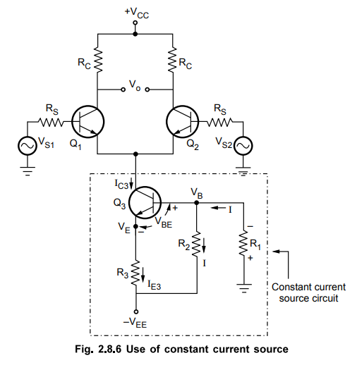
The
transistor used is Q3 and the values of R1, R2
and R3 are selected so as to give the same operating point values
for the two transistors Q1 and Q2.
a.
Circuit Analysis
Let
current through R3 be IE3 while current through R1
is I.
Neglecting
the base current of Q3 which is very small due to large βac,
we can assume that current through R2 is also I.
Applying
Kirchhoff's voltage law,
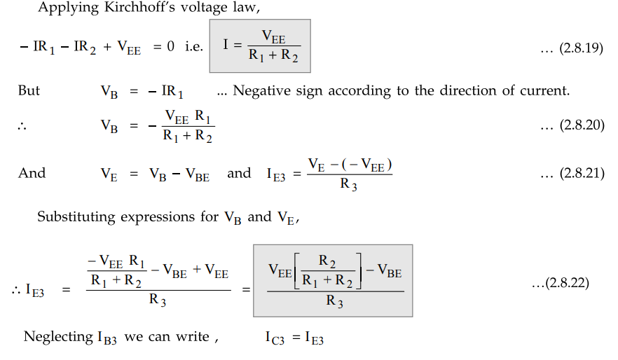
Thus
as VEE , R1, R2, R3 and VBE
are constants, current IC3 is almost equal to IE3 and
also constant. Thus circuit with transistor Q3, acts as a constant
current source.
Key
Point The internal resistance of a constant current
source is very high, ideally infinite. Hence this circuit makes the value of
emitter resistance ideally infinite which reduces the common mode gain Ac
ideally to zero. Thus as Ac tends to zero, CMRR tends to infinite.
Review Questions
1. Using the h-parameters, carry out the a.c. analysis of the differential
amplifier. Find Ad, Ac , Ri and Ro
for dual input balanced output.
2. The parameters for the differential amplifier are given as :
RC = 1 k Ω , RS = 1 k Ω , hfe= 1 k Ω and RE = 2 M Ω Neglecting hoe, calculate the difference mode gain
and common mode gain. Hence calculate CMRR in dB. The amplifier is in dual
input, balanced output configuration.
[ Ans.: 100.17 dB ]
3. For the differential amplifier shown in the Fig. 2.8.7,
determine
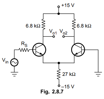
i) The voltages at the collector of each transistor
ii) The differential voltage gain.
Assume VBE = 0.7 V, hfe =100, hie
= 3.9 k Ω and the source resistance as 1 k Ω
[ Ans.: 13.2 V, 34.69 ]
4. Draw the circuit of a symmetrical emitter coupled
differential amplifier and derive the expression for the CMRR.
5. How common mode rejection ratio can be increased using
constant current source ?
Linear Integrated Circuits: Unit II: Characteristics of Op-amp : Tag: : Working Principle, Mode Operation, Circuit Diagram, Solved Example Problems | Op-amp - A.C. Analysis of Differential Amplifier using h-Parameters
Related Topics
Related Subjects

Linear Integrated Circuits
EE3402 Lic Operational Amplifiers 4th Semester EEE Dept | 2021 Regulation | 4th Semester EEE Dept 2021 Regulation