Linear Integrated Circuits: Unit IV: Special ICs
AD633 Multiplier IC
Operating working principle, Features, Functional Block Diagram, Pin Diagram, Application Circuits
The IC AD633 is a multiplier IC by analog devices. It is low cost, 8 pin, 4 quadrant multiplier IC. The various features of AD633 are,
AD633 Multiplier IC
The
IC AD633 is a multiplier IC by analog devices. It is low cost, 8 pin, 4
quadrant multiplier IC.
The
various features of AD633 are,
1.
It is complete four quadrant multiplier.
2.
No external components or expensive user calibration is necessary.
3.
It is low cost and easy to use.
4.
It is highly stable and reliable because of monolithic construction and laser
calibration.
5.
It has differential high impedance X and Y inputs. The input impedance is as
high as 10 MΩ.
6.
The internal reference is generated by very stable zener diode hence accuracy
is not supply sensitive. The scaling reference is 10 V.
7.
The total accuracy is 2 % of full scale.
8.
It has 1 MHz bandwidth, 20 V/gsec of slew rate and ability to drive capacitive
loads.
9.
The Z input provides access to the output buffer amplifier, enabling the user
to sum the outputs of two or more multipliers, increase the multiplier gain,
convert the output voltage to current and configure variety of application
circuits.
1. Functional Block Diagram
The
Fig. 4.10.1 shows the functional block diagram of AD633.
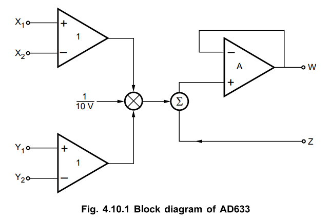
There
are two differential inputs X and Y where X = X1 - X2 while
Y = Y1-Y2. These inputs are converted to the currents by
voltage to current converters. The product of these currents is than generated.
A buried zener reference generates on overall scale factor of 10 V. Thus the
product X + Y / 10 is applied as one input to the summer while Z is another
input to the summer. The signal (X+Y / 10 +Z) is applied to the output amplifier to produce
output W. The amplifier summing node Z allows the user to add two or more
multiplier outputs, convert the output voltage to current and configure various
analog computational functions.
The
overall transfer function is,
The
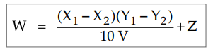
Fig. 4.10.2 shows the pin diagram of AD633 multiplier IC. ± VS are the supply
pins.
The
various applications of AD633 include multiplication, division, squaring,
modulation, demodulation, phase detection, attenuators, filters, voltage
controlled amplifier etc.
2. Application Circuits
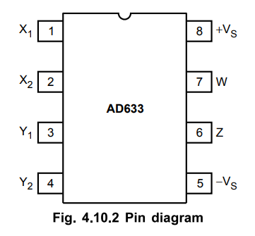
1.
Squaring circuit
The
Fig. 4.10.3 shows use of AD633 as a squaring circuit
The
output polarity can be reversed by interchanging the X and Y inputs.
2.
Frequency doubler circuit
For
frequency doubling without d.c. term, RC network is used at the input as shown
in the Fig. 4.10.4.
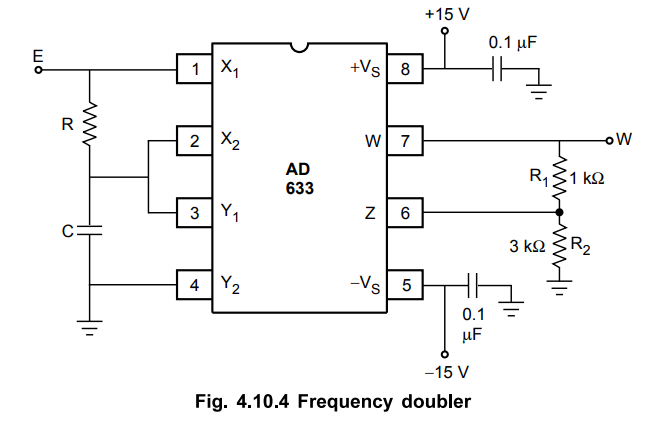
At
ω, the X input leads the input voltage by 45° and is attenuated by 1/ √2.
TheY input lags the X input by 45° and also attenuated by 1/ √2.
Thus the X and Y inputs are 90° out of phase. When E is sine wave as E sin ω t
then,
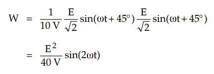
The
resistors R1 and R2 are included to restore the output
amplitude to 10 V for an input amplitude of 10 V.
3.
Variable scale factor
For
getting a scale factor other than 10, the circuit shown in the Fig. 4.10.5 can
be used.
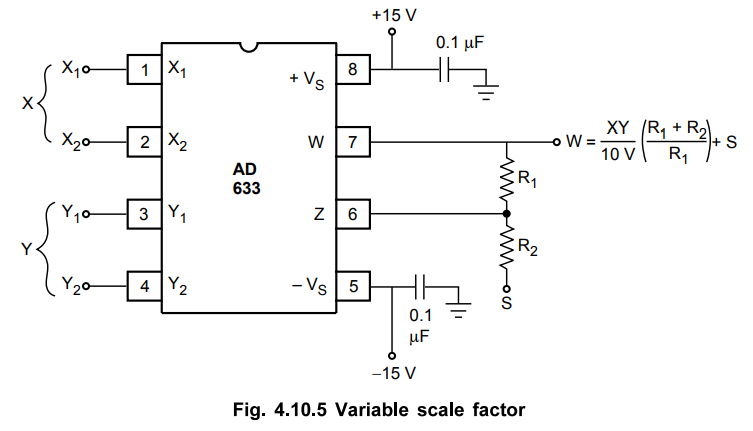
The
potential divider at the output increases the scale factor by R1 + R2
/ R1. Practically it can be limited upto 100. The summing input S
can be used to add additional signal or otherwise it can be grounded.
Review Questions
1. Write a detailed
note on AD633 multiplier.
2. Explain any two
applications of AD633 multiplier.
Linear Integrated Circuits: Unit IV: Special ICs : Tag: : Operating working principle, Features, Functional Block Diagram, Pin Diagram, Application Circuits - AD633 Multiplier IC
Related Topics
Related Subjects

Linear Integrated Circuits
EE3402 Lic Operational Amplifiers 4th Semester EEE Dept | 2021 Regulation | 4th Semester EEE Dept 2021 Regulation