Linear Integrated Circuits: Unit III: Applications of Op-amp
ADC (Analog to Digital Converter) using Op-amp
Performance Parameters, Working Principle, Circuit Diagram, Types, Solved Example Problems | Operational amplifier
The A/D conversion is a quantizing process whereby an analog signal is converted into equivalent binary word. Thus the A/D converter is exactly opposite function that of the D/A converter.
A/D Converters
May-03,04,05,06,07,08,09,10,11,12,14,16,18,
Dec.-03,04,05,06,07,08,09,10,ll,16
The
A/D conversion is a quantizing process whereby an analog signal is converted
into equivalent binary word. Thus the A/D converter is exactly opposite
function that of the D/A converter.
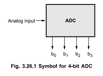
Fig.
3.26.1 shows symbol for A/D converter.
1. Performance Parameters of ADC
The
Fig. 3.26.2 shows the digital output of an ideal 3 bit ADC plotted against the
analog input voltage.
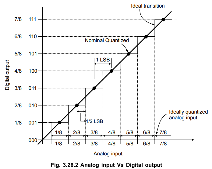
a.
Resolution
Fig.
3.26.2 shows eight (23) discrete output states from 0002
to 1112, each step being 1/8 V
apart. Therefore, we can say that expression of ADC resolution is the same as
for 8 the DAC and is repeated here :
Resolution
= 2n ... (3.26.1)
Resolution
is also defined as the ratio of a change in value of input voltage, V,-, needed
to change the digital output by 1 LSB. If the full scale input voltage required
to cause a digital output of all l's is ViFS, then resolution can be
given as
b.
Quantization Error
Fig.
3.26.2 shows that the binary output is 011 for all values of Vi
between 1/4 and 1/2 Vi. There is an unavoidable uncertainty about
the exact value of Vi when the output is 011 This uncertainty is
specified as quantization error. Its value is ± 1/2 LSB.
It
is given as, QE = ViFS / (2n – 1)2 …. (3.26.3)
Increasing
the number of bits results in a finer resolution and a smaller quantization
error. The quantization error can be observed by continuously sampling a
time-varying analog signal with an ADC, converting it back to analog with a
DAC, and taking the difference between the two. The resulting sawtooth-like
signal, called quantization noise.
The
root mean square value of such signal, En can be given as
En
= VFS / 2n √12
This
is related to the resolution of the system. For each additional bit of
resolution En is cut in half, that is reduced by 6 dB.
c.
Accuracy
Absolute
accuracy is the maximum deviation between the actual ADC output and the ideal
ADC output. The relative accuracy is the maximum deviation after gain and
offset errors have been removed. The data sheet of ADC includes the relative
accuracy.
d.
Linearity
It
is an important parameter of the accuracy of ADC. It indicates how close the
ADC output is to its ideal transfer characteristics.
e.
Settling Time
It
is the time taken by the output of ADC to settle within a specified band ±(1/2)
LSB
of its final value following a code change at the input (generally a full scale
change).
f.
Specifications of Sample and Hold Circuit
For
accurate analog to digital conversion the analog input voltage should be held
constant during the conversion cycle. The sample and hold circuit does this
task. The specifications of sample and hold circuit are explained below with
the help of waveform of sample and hold circuit.
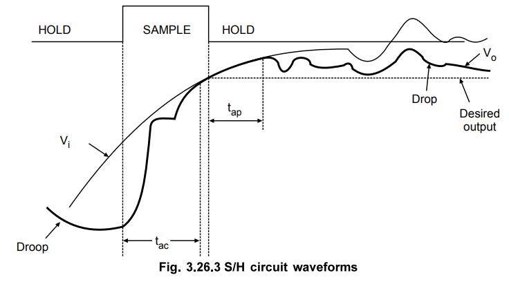
1.
Acquisition time (tac)
It
is the time required for the holding capacitor CH to charge up to a level close
to the input voltage during sampling. It depends on three factors :
•
RC time constant
•
Maximum output current of op-amp
•
Slew rate of op-amp
2.
Aperture time (tap)
Because
of propagation delays through the driver and switch, Vo will keep
tracking Vi some time after the inception of the hold command. This
is the aperture time. To get the precise timing, it is necessary to advance
hold command by this amount.
3.
Aperture uncertainty (Δ tap)
It
is the variation in aperture time from sample to sample. Due to aperture
uncertainty it is difficult to compensate aperture time by advancing hold
command.
4.
Code width
The
code width is the change in input voltage that occurs between the output code
transitions expressed in LSBs of full scale. Code width uncertainty is the
dynamic variation or jitter in the code width causing noise.
Example
3.26.1 An 8-bit ADC outputs all l's when Vi -5.1
V. Find its a) Resolution and b) Digital output when V i - 1.28 V.
Solution
:
a) Resolution = 2n = 28 = 256
and
resolution = 5.1 V / 28 – 1 = 20 mV/LSB
Therefore,
we can say that to change output by 1 LSB we have to change input by 20 mV.
b)
For 1.28 V analog input, digital output can be calculated as,
D
= 1.28 V / 20mV / LSB = 64 LSBs
The
binary equivalent of 64 is 0100 00002
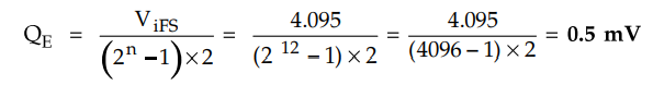
Example
3.26.2 Calculate the quantizing error for 12-bit ADC
with full scale input voltage 4.095 V.
Solution
:
2. Basic Conversion Techniques
Analog
to digital converter are classified into two general groups based on the
conversion techniques. One technique involves comparing a given analog signal
with the internally generated reference voltages. This group includes
successive approximation, flash, delta modulated (DM), adaptive delta modulated
and flash type converters. The another technique involves changing an analog
signal into time or frequency and comparing these new parameters against known
values. This group includes integrator converters and voltage-to-frequency
converters.
In
this chapter we are going to discuss following types of ADCs using various
conversion techniques :
1.
Single ramp or single slope
2.
Dual slope
3.
Successive approximation
4.
Flash
5.
Delta modulation
6.
Adaptive delta modulation
a.
Dual Slope ADC
Dual
slope conversion is an indirect method for A/D conversion where an analog
voltage and a reference voltage are converted into time periods by an
integrator, and then measured by a counter. The speed of this conversion is slow
but the accuracy is high.
Fig.
3.26.4 shows a typical dual slope converter circuit. It consists of integrator
(ramp generator), comparator, binary counter, output latch and reference
voltage. The ramp generator input is switched between the analog input voltage
and a negative reference voltage, -VREF. The analog switch is
controlled by the MSB of the counter. When the MSB is a logic 0, the voltage
being measured is connected to the ramp generator input. When MSB is logic 1,
the negative reference voltage is connected to the ramp generator.

At
time t = 0, analog switch S is connected to the analog input voltage Vp so that
the analog input voltage integration begins. The output voltage of the
integrator can be given as,
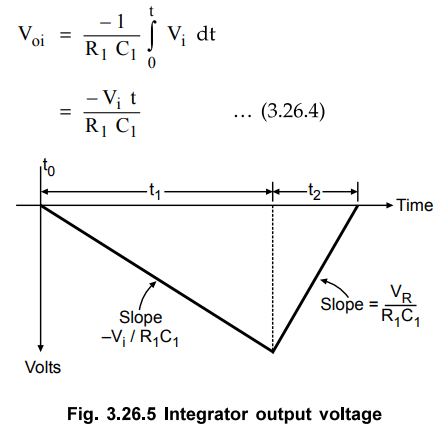
where
R1 C1 is the integrator time constant and V is assumed
constant over the integration time period. At the end of 2N clock periods MSB
of the counter goes high. At a result the output of the flip-flop goes high,
which causes analog switch S to be switched from Vi to -VR. At this
very same time the binary counter which has gone through its entire count
sequence is reset. If the clock period is T, the integration takes place for a
time tF = 2n × T. At the end
of t1 the output voltage Vo is given by
Vo
= V1 = - (1 / R1C1) Vi ti
The
negative input voltage (-VR) connected to the input of integrator
causes the integrator output to ramp positive. When integrator output reaches
zero, the comparator output voltage goes low, which disables the clock AND
gate. This stops the clock pulses reaching the counter, so that the counter
will be stopped at a count corresponding to the number of clock pulses in time
t2.
t2
= Count / Clock rate and Vl =
1/ RC (-VR)t2
The
integrator output ramp down to a voltage V and get back upto 0. Therefore, the
charge voltage is equal to discharge voltage and we can write,
The
above equation shows that t2 is directly proportional only to the Vi
since VR and t1 are constants. The binary digital output
of the counter gives corresponding digital value for time period t2
and hence it is also directly proportional to input signal Vi
The
actual conversion of analog voltage Vin into a digital count occurs
during t2. The control circuit connects the clock to the counter at
the beginning of t2. The clock is disconnected at the end of t2.
Thus the counter contents is digital output. Hence we can write,
Digital
output = (Counts / Second) t2 … (3.26.6)
But
from equation (3.26.5) we can write,
Digital
output = (Counts / Second) t1 (Vi / VR) … (3.26.7)
The
counter output can then be connected to an appropriate digital display.
The
advantages of dual slope ADC are,
1.
It is highly accurate.
2.
Its cost is low.
3.
It is immune to temperature caused variations in R1 and C1.
4.
It avoids the drift problem because both the integrator gain and the counting
rate do not vary between two phases t1 and t2
The
only disadvantage of this ADC is its speed which is low.
b.
Successive Approximation ADC
In
this technique, the basic idea is to adjust the DAC's input code such that its
output is within ± 1/ 2 LSB of the analog input Vi to be A/D
converted. The code that achieves this represents the desired ADC output.
The
successive approximation method uses very efficient code searching strategy
called binary search. It completes searching process for n-bit conversion in
just n clock periods.
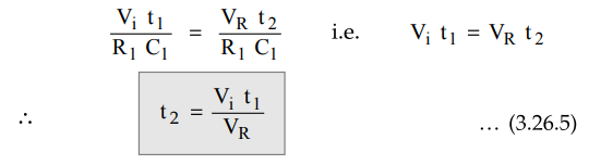
Fig.
3.26.6 shows the block diagram of successive approximation A/D converter. It
consists of a DAC, a comparator, and a successive approximation register (SAR).
The
external clock input sets the internal timing parameters. The control signal
start of conversion (SOC) initiates an A/ conversion process and end of conversion
signal is activated when the conversion is completed.
Operation :
The
searching code process in successive approximation method is similar to
weighing an unknown material with a balance scale and a set of standard
weights. Let us assume that we have 1 kg, 2 kg and 4 kg weights (SAR) plus a
balance scale (comparator and DAC). Now we will see the successive
approximation analogy for 3-bit ADC.
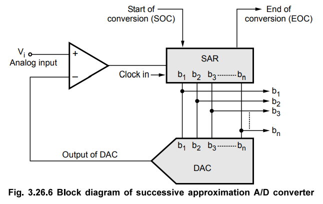
Refer Fig. 3.26.6 and 3.26.7. The analog voltage Vin is applied at one input of comparator. On receiving start of conversion signal (SOC) successive approximation register sets 3-bit binary code 1002 (b2 =1) as an input of DAC. This is similar process of placing the unknown weight on one platform of the balance and 4 kg weight on the other. The DAC converts the digital word 100 and applies it equivalent analog output at the second input of the comparator. The comparator then compares two voltages just like comparing unknown weight with 4 kg weight with the help of balance scale. If the input voltage is greater than the analog output of DAC, successive approximation register keeps b2 = 1 and makes b1 = 1 (addition of 2 kg weight to have total 6 kg weight) otherwise it resets b2 = 0 and makes b1 = 1 (replacing 2 kg weight). The same process is repeated for b1 and bo. The status of b0, b1 and b2 bits gives the digital equivalent of the analog input. Fig. 3.26.7 illustrates the process we have just discussed.
The
dark lines in the Fig. 3.26.7 shows setting and resetting actions of bits for
input voltage 5.2 V, on the basis of comparison. It can be seen from the Fig.
3.26.7 that one clock pulse is required for the successive approximation regsiter
to compare each bit. However an additional clock pulse is usually required to
reset the register prior to performing a conversion.
The
time for one analog to digital conversion must depend on both the clock's
period T and number of bits n. It is given as,
TC
= T (n + 1) ...(3.26.8)
where
TC = Conversion time, T = Clock period, n = Number of bits
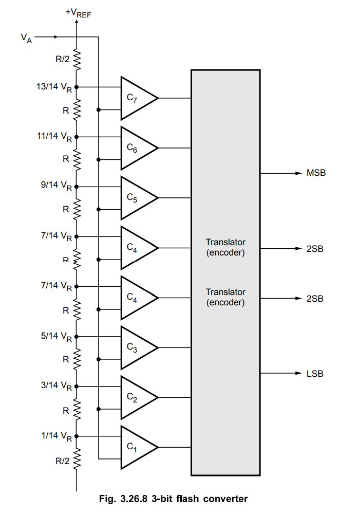
c.
Flash ADC
When system designs call for the highest speed available, flash-type A/D converters (ADCs) are likely to be the right choice. They get their names from their ability to do the conversion very rapidly. Flash A/D converters, also known as a simultaneous or parallel comparator ADC, because the fast conversion speed is accomplished by providing 2n - 1 comparators and simultaneously comparing the input signal with unique reference levels spaced 1 LSB apart.
Fig.
3.26.8 shows 3-bit flash A/D converter. For this ADC, seven (23 -1)
comparators are required. As shown in the Fig. 3.26.8, one input of each
comparator is connected to the input signal and other input to the reference
voltage level generated by the reference voltage divider. The reference voltage
(VREF) is equal to the full scale input signal voltage. The manner
in which the flash A/D converter performs a quantization is relatively simple.
The
comparators give output "1" or "0" state depending on
whether the input signal is above or below the reference level at that instant.
Those comparators referred above the input signal, remain tumed-off,
representing a "0" state. The comparators at or below the input
signal conversely become a "1" state. The code resulting from this
comparator is converted to a binary code by the encoder.
The
number of comparators required for n bit resolution is,
Number
of comparators = 2n – 1 ... (3.26.9)
As
seen earlier the quantization error is ± 2 LSB. Thus for an ADC, the maximum frequency
for a sine wave to be digitised within an accuracy of ± 2 LSB is,
fmax
≅
1/ 2π(TC)2n ...
(3.26.10)
where
fmax = Maximum input frequency
TC
= Conversion time and n = Number of bits
d.
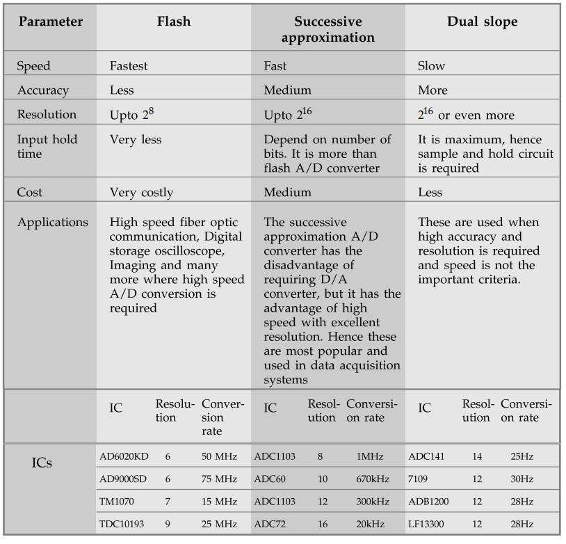
Comparison between Flash, Dual Slope and Successive Approximation Techniques
The
comparison of ADCs is given in the tabular form as below :
Example
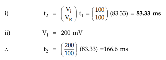
3.26.3 For a particular dual slope ADC, t1is
83.33 ms and the reference voltage is 100 mV. Calculate t2 if i) Vi
is 100 mV and ii) 200 mV.
Solution
:
We know that,
Example
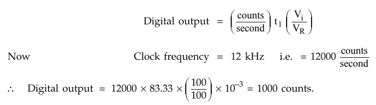
3.26.4 Find the digital output of an ADC having t1
as 83.33 ms and VR as 100 mV for an input voltage of +100 mV. The
clock frequency is 12 kHz.
Solution
:
The digital output is given as,
Example
3.26.5 An 8 bit successive approximation ADC is driven by a
1 MHz clock. Find its conversion time.
Solution
:
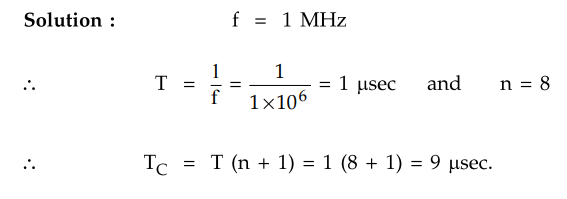
Example
3.26.6 For a particular 8-bit ADC, the conversion time
is 9 μs. Find the maximum frequency of an input sine wave that can be
digitized.
Solution:
The maximum frequency is given by,
fmax
≈ 1 / 2π(TC)2n ≈ 1 / 2π × 9 × 10-6 × 28
= 69.07 Hz
Example
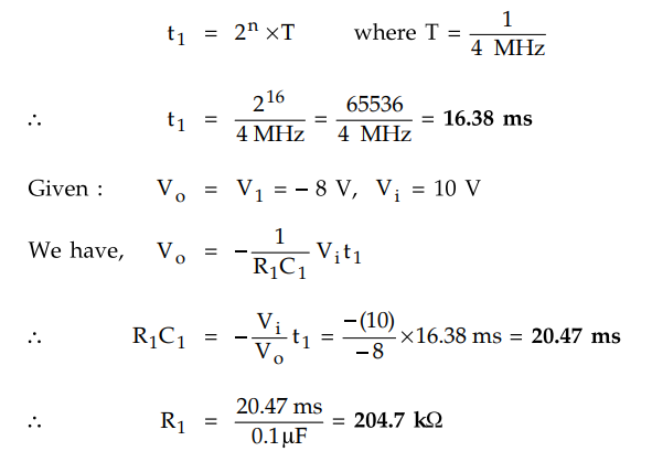
2.26.7 A dual slope ADC uses 16-bit counter and 4 MHz
clock rate. The maximum input voltage is + 10 V. The maximum integrator output
voltage should be - 8 V when the counter has cycled through 2n counts.
The capacitor used in the integrator is 0.1 µF . Find the value of resistor R
of the integrator.
Solution
:
e.
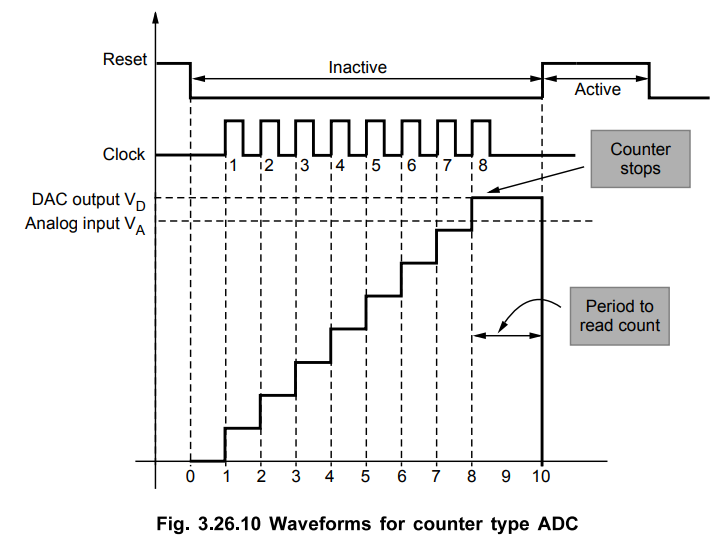
Counter Type ADC
Principle of operation :
This
ADC uses DAC for A to D conversion. The output of the DAC is continuously
compared with the analog input to the ADC which is to be converted into digital
output. When the output of the DAC becomes greater than this analog input, the
corresponding digital input to the DAC is noted which represents the analog
input to the ADC.
Fig.
3.26.9 shows the circuit diagram of counter type ADC.
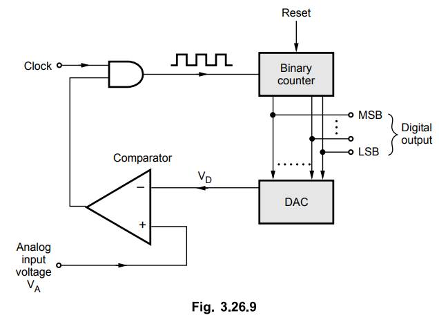
As
shown in the Fig. 3.26.9, the counter type ADC consists of a binary counter,
DAC, comparator and AND gate. The operation of the circuit is explained below.
i)
Initially, the counter is reset, i.e. its output is set to zero by applying a
reset pulse. The output of the counter is given as digital input to DAC. Since
input to DAC is zero, its output VD is zero.
ii)
When the analog input voltage VA is applied to ADC, it becomes
greater than VD - VA acts as input voltage for non
inverting terminal and VD acts as input voltage for inverting
terminal of the comparator. Since VA is greater than VD,
the comparator output goes high.
iii)
For an AND gate, one input is clock pulses and another input is the output of
the comparator. Because of the high output of the comparator, the clock pulses
are allowed to pass through the AND gate.
iv)
The counter starts counting these close pulses. According to the number of
clock pulses, the output of the counter goes on increasing. This increases the
output of the DAC.
v)
The above steps are continued till VD is less than VA.
vi)
As soon as DAC output VD becomes greater than VA, the
comparator output goes low. This disables AND gate. So the clock pulses are not
allowed to pass through the AND gate. The counting process of the binary
counter is stopped.
vii)
The output of the binary counter which is in digital form is noted which
represents the digital equivalent of the analog input voltage VA
viii)
For the next A to D conversion, the input voltage to ADC, VA
changes. The binary counter is cleared by applying a second reset pulse and all
the above steps are repeated to obtain the digital equivalent of VA.
Disadvantages
It
is necessary to give enough time for DAC conversion and comparator to respond.
Therefore, there is a limitation on the clock frequency. As clock frequency is
low, the speed of conversion is less.
Conversion
time is not constant. It increases with increase in input voltage. In other
words, we can say that conversion time is high at high input voltage.
Review Questions
1. Explain in detail
about successive approximation ADC.
Dec.-03, 09, 12, 16,
May-06, 07, 12, 16, 18, Marks 12
2. With neat diagram
explain the working of dual slope type ADC.
Dec.-03, 04, 06,11,
May-08, 10, 14, Marks 8
3. Explain any two
techniques of converting analog to digital signal.
4. Compare the
performances of various types of ADC.
5. Explain the
functions of flash type A/D converter.
6. Explain the
following characteristics of ADC resolution, accuracy, settling time,
linearity.
May-10, Marks 8
7. What are the
advantages of continuous type A/D converter over counter type A/D converter ?
May-18, Marks 2
Linear Integrated Circuits: Unit III: Applications of Op-amp : Tag: : Performance Parameters, Working Principle, Circuit Diagram, Types, Solved Example Problems | Operational amplifier - ADC (Analog to Digital Converter) using Op-amp
Related Topics
Related Subjects

Linear Integrated Circuits
EE3402 Lic Operational Amplifiers 4th Semester EEE Dept | 2021 Regulation | 4th Semester EEE Dept 2021 Regulation