Linear Integrated Circuits: Unit IV: Special ICs
Analog Multiplier IC
Characteristics, Symbol, Block Diagram, Pin Diagram, Performance Parameters, Applications
Monolithic Integration has lowered the cost of multiplier ICs considerably. Such an IC is not only useful as multiplier but can be used as a simple and direct solution to complex signal processing problems.
Analog Multiplier IC
The
multiplier integrated circuit is commonly used in practice to perform various
mathematical operations.
Monolithic
Integration has lowered the cost of multiplier ICs considerably. Such an IC is
not only useful as multiplier but can be used as a simple and direct solution
to complex signal processing problems. Such ICs can be configured to use in many
applications as signal multiplications in process instrumentation, chemical
analyzers, servo mechanism control systems, frequency doublers, phase angle
detectors, true r.m.s. converter, controlling of oscillator frequency and so
on. The ICs can be used to improve the data acquisition through ratioing two
signals. Let us study first a basic multiplier IC and its characteristics.
1. Basic Multiplier and its Characteristics
A
basic multiplier is an active circuit in which the output voltage is proportional
to the product of the two input signals. A schematic symbol of such basic
multiplier IC is shown in the Fig. 4.8.1.
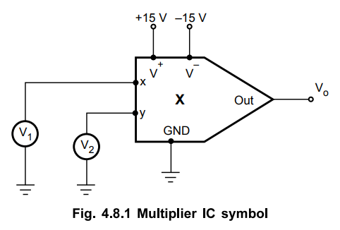
The
terminals V+ and V- are supply terminals for IC where
dual supply is to be connected, generally ± 15 V as shown. The x and y are the
two input terminals where two inputs V1 and V2 are
connected.
The
output of such basic multiplier is
Vo
= K V1 V2 ...
(4.8.1)
where
K is constant and is equal to 1 / Vref Usually Vref is
set to 10 V internally and hence,
Vo
= V1 V2 / 10 ... (4.8.2)
As
long as it is ensured that both the input voltages are below the reference
voltage, (V1 V2 <
Vref ), the output of the basic multiplier will not saturate.
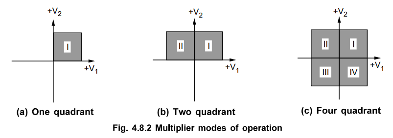
Depending
on the use of the basic multiplier, it is necessary to restrict the polarity of
one or both the inputs. Depending upon the polarity restriction, the IC
operation is called as,
i)
One quadrant multiplier : In such operation, the polarities
of both the inputs must always be positive.
ii)
Two quadrant multiplier : A two quadrant multiplier functions
properly if one input is held positive and the other is allowed to swing in
both positive and negative.
iii)
Four quadrant multiplier : If both the inputs are allowed to
swing in both positive and negative directions, the operation is four quadrant
multiplier operation.
These
operations are shown in the Fig. 4.8.2.
Performance
Parameters of Multiplier
Let
us define the performance parameters of a multiplier.
1.
Accuracy : It is the maximum deviation of the actual output
level from the ideal one. This deviation is also called total error. It is
generally specified interms of percentage of full scale output.
2.
Linearity : It is the maximum output deviation from
the best fit straight line at the output, where one input is varied from end to
end while the other is kept fixed, usually at + 10 V or - 10 V. It is also
expressed interms of percentage of full scale output.
3.
Bandwidth : It is the range upto the frequency
where the output is 3 dB below its low frequency value. This is also called as
small signal bandwidth. It depends on the active device used.
4.
1 % absolute error bandwidth : It represents the
frequency where the output magnitude starts to deviate from its low frequency
value by one percent.
5.
Feed through voltage : It is the peak to peak voltage at
the output when one of the two inputs is grounded. As the output is the
multiplication of the two inputs,
if
one of the inputs is made zero, the output of ideal multiplier also must be
zero. But in practice, there exists a small voltage at the output. This voltage
is different for the two input terminals.
6.
Zero trim : It is the ability of the multiplier to
set the feed through voltage at the output to zero.
7.
Scale factor : It is the proportionality constant (K)
relating the output voltage and the product of the two input voltages.
K
= Vo / V1 V2
... (4.8.3)
8.
Quadrant : This indicates the restriction on the polarities of
the two input voltages. For one quadrant operation, both the inputs must be
positive, for two quadrant one must be positive while the other can be bipolar.
And for the four quadrant operation, both the inputs can be bipolar.
2. Applications of Multiplier
The
multiplier is used in many practical applications. Some of these applications
are:
1.
In communication it is used in amplitude modulation, phase modulation,
frequency modulation, phase detection, suppressed carrier modulation etc.
2.
In instrumentation and control used to measure velocity, acceleration,
instantaneous power, automatic gain control, etc.
3.
For voltage controlled attenuators and for voltage controlled amplification.
4.
It is used for voltage divider, true r.m.s calculation, rectifier phase shift
detection etc.
5.
It is used for frequency converters, frequency doubling and frequency shifting
etc.
6.
It is used for squaring and square root calculations.
7.
It is used to solve nonlinear equations.
8.
It is used in oscillators to generate the waveforms and also used for square
wave generation etc.
Let
us discuss, few of these applications in detail along with the circuit diagram
and the operation.
a.
Voltage Divider using Multiplier
The
circuit in which output is the division of the two input signals, is called as
a voltage divider. The use of multiplier as a voltage divider is shown in the
Fig. 4.8.3.
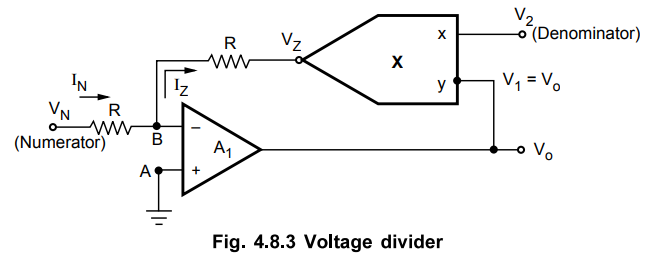
The
multiplier is used in the feedback loop. The denominator is applied at the x
input of the multiplier which is the voltage V2. The numerator is
applied at the input terminal of op-amp A1.
As
node A is grounded, node B is also at virtual ground, hence VB = 0. As op-amp
input current is zero,
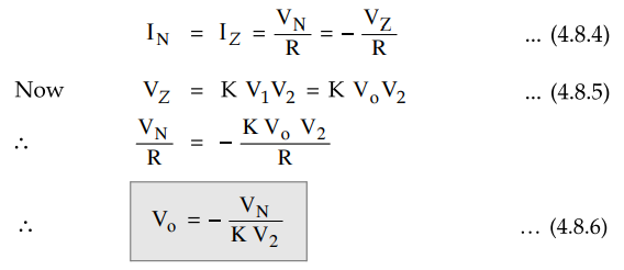
Thus
the output is proportional to the division of the two input voltages VN
and V2. The only requirement is that the input voltage V2
must be negative. Hence divider circuits are at best two quadrant circuits.
b.
Squaring Circuit using Multiplier
The
squaring circuit gives square of the input voltage applied. The multiplier
inputs are connected together to get the squaring circuit as shown in the Fig.
4.8.4.
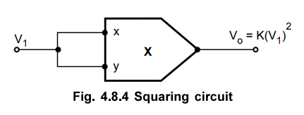
The
same signal V1 is applied to both the input terminals of the
multiplier.
So
V2 = V1 and hence
the output of the multiplier is,
Vo
= K V1 V2 = K (V1)2
….. (4.8.7)
Thus
the output is proportional to the square of the input.
c.
Square Rooting Circuit using Multiplier
Similar
to the squaring, the square rooting circuit can be obtained using multiplier. The
circuit is shown in the Fig. 4.8.5.
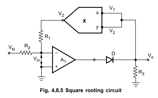
A
multiplier configured as squaring circuit is used in the feedback loop. The
gain of the op-amp A1 is say A and voltage between inverting a nd
non-inverting terminal is Vin. So we can write,
Vo
= - Vin × A
Vin
= - Vo / A ….. (4.8.8)
Now
the voltage Vin is composed of two components, one that of VZ and
other that of VN.
As
seen from the equation (4.8.13), the output is proportional to the square root
of VN, but the VN must be always negative, (VN
< 0). Otherwise the circuit becomes latched up and normal operation can only
be restored by breaking the feedback loop. To avoid such problem, a series
diode D is provided.
d.
Frequency Doubler using Multiplier
The
multiplication of two sine waves of same frequency but of possibly different
amplitudes and phases, gives us a signal of a double frequency.
Consider
the two input signals as,
V1
= V1m sin ω t and V2 = V2m sin (ω t + θ )
When
the two inputs are given to a multiplier we get,
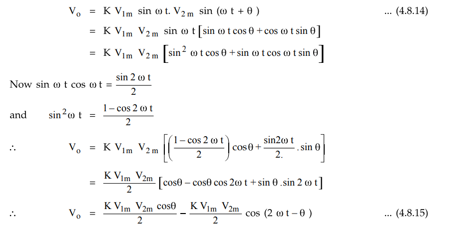
The
first term is D.C. for a phase difference of θ while the second term varies
with time but at twice the frequency of the inputs. Thus circuit acts as a
frequency doubler.
Such
a frequency doubler can be obtained by using a squaring circuit, as shown in
the Fig. 4.8.6.
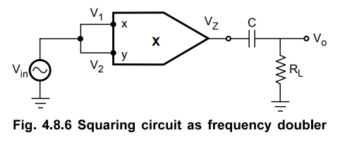
The
two inputs are connected together hence
V1
= V2 = Vin = Vm sin ω t
Here
θ = 0° which is phase difference between the two inputs.
Thus
the output of the multiplier is the D.C. signal with time varying signal of
double the input frequency.
The
capacitor C connected in series with the output blocks the D.C. and removes it.
Thus we get,
Thus
the circuit acts as a frequency doubler.
e.
Phase Angle Detection using Multiplier
The
frequency doubler circuit with two inputs of same frequency but different
amplitudes and v phases can be used to obtain the phase angle detection
circuit, as shown in the Fig. 4.8.7.
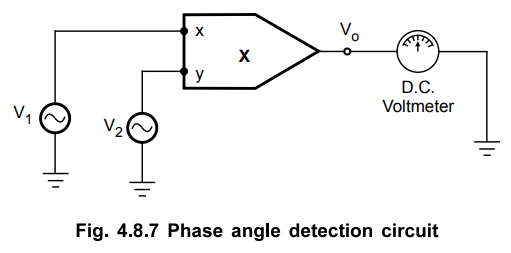
As seen earlier, the output of the multiplier is
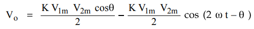
This
is because, circuit acts as a frequency doubler. Now the D.C. voltmeter is
connected at the output. The voltmeter will not respond to a.c. component
present in the output, while the d.c. component can be easily measured on the
voltmeter.
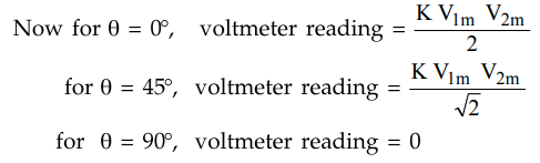
So
calibrating the d.c. voltmeter as a phase angle meter, the phase angle between
the two inputs can be measured.
f.
RMS Detector
The
RMS value of a signal is given by,
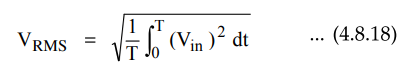
The
operation is performed in reverse order as squaring, finding the mean i.e.
integrating and finally finding the square root. The Fig. 4.8.8 shows the basic
circuit for the RMS detector.
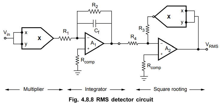
The
circuit has a multiplier as a squaring device as its first element. This gives
square of the input, the op-amp A1 is an integrator which gives the integration
of squared input. Finally op-amp A2 along with the multiplier in its feedback
loop performs square rooting operation, on the output of op-amp A1. Thus the
final output is the RMS value of the input applied.
g.
Rectifier using Multiplier
A
full wave rectifier circuit using multiplier is shown in the Fig. 4.8.9.
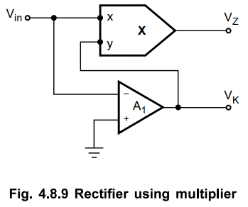
The
op-amp A1 is used as a non-inverting comparator. The output of
op-amp A1 is VK and which is at ± Vsat
depending upon whether the input Vin is positive or negative.
The
multiplier used is a four quadrant multiplier whose output is always positive.
Hence we get the full wave rectified signal at Vz while the square wave
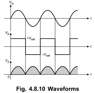
signal at VK. The waveforms are shown in the Fig. 4.8.10.
Key
Point As the output of the multiplier is always
positive, the circuit is also called as absolute value circuit.
3. Study of Multiplier ICs
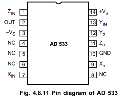
a.
Study of Multiplier ICs AD 533
The
IC AD 533 is a multiplier IC by Analog Devices. It is a low cost integrated
circuit comprising a transconductance multiplying element, stable reference and
an output amplifier, on a monolithic silicon chip.
The
various features of AD 533 are :
1)
Its operation is very simple.
2)
Only four external adjustments are necessary.
3)
Maximum four quadrant error is below 0.5 %.
4)
Its temperature drift is as low as 0.01 %/ °C
5)
It is suitable for the applications like multipliers, dividers, square and
square root extractor circuits etc, alongwith the operational amplifier.
The
specified accuracy for the multiplifer can be easily achieved, by the straight
forward adjustment of feedthrough, output zero and gain trim pots.
The
scale factor of AD 533 is 1/10 for four quadrant operation hence it multiplies
in four quadrants with a transfer function of XY/10. It divides in two
quadrants with a transfer function of 10Z/X. While it calculates square root
with a transfer function of -√10Z.
All
models of AD 533 are available in hermetically sealed TO-100 and metal can
packages or TO-116 ceramic DIP packages. The pin diagram of AD 533 is shown in
the Fig. 4.6.11.
AD
533, for operation from -55 °C to +125 °C, has a maximum 1 % error in
multiplying, at 25 °C.
The
op-amp output provides ± 10 V at 5 mA and is fully protected against short
circuits to ground or either supply voltage. All the inputs are fully protected
against over voltage transients.
The
device has excellent a.c. performance with typical small signal bandwidth of 1
MHz and the slew rate of 45 V/µsec.
The
low cost and simplicity of operation of the AD 533 make it especially well suited
for use in the widespread applications such as,
1)
Function generation
2)
Peak detection
3)
RMS compution
4)
Automatic gain control
5)
Frequency discrimination
6)
Phase detection
7)
Square and square root extractor
8)
Modulation and demodulation
Use
of AD 533 is some of the basic applications is discussed here.
1.
AD 533 as Multiplier
The
connection diagram of AD 533 as a multiplier, alongwith the component values is
shown in the Fig. 4.8.12.
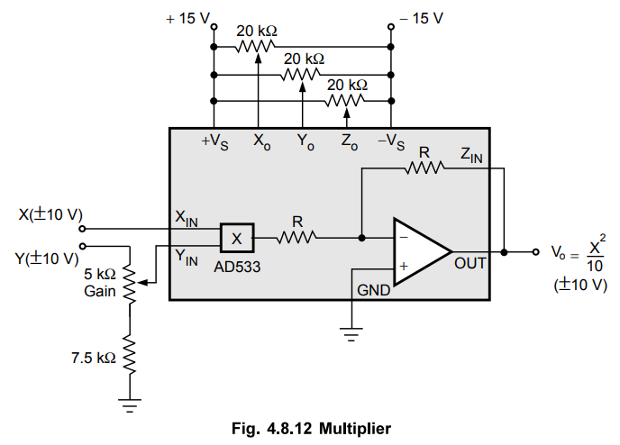
The
multiplier operation is possible by closing the loop around the internal op-amp
with the Z input connected to the output.
The
Xo null pot balances the X input channel to minimize Y feedthrough and the Yo
null pot balances the Y input to minimize X feedthrough. The Zo pot
compensates the output op-amp offset voltage. The gain pot sets the full scale
output level.
The
output is given by,
Vo
=XY / 10
2.
AD 533 as Squarer
The
connection diagram of AD 533 as a squarer alongwith the component values is
shown in the Fig. 4.8.13.
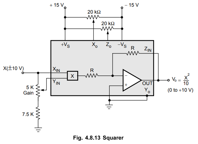
The
squarer is a special case of multiplier operation where both the input X and Y
are connected together and two quadrant operation results. The output is always
positive. When the X and Y inputs are connected together then combined offset
which is algebraic sum of the individual offsets, results. This can be nulled
using the Xo pot alone. The output is given as,
Vo
= XY / 10 = X2 / 10
3.
AD 533 as Divider
The
connection diagram of AD 533 as divider is shown in the Fig. 4.8.14.
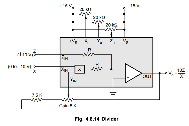
The
divide mode utilises the multiplier in a fedback configuration where the Y
input now controls the feedback factor. With X = full scale, the gain Vo
/Z becomes unity after trimming. Reducing the X input, reduces the feedback
around the op-amp by a like amount, thereby increasing the gain. This
reciprocal relationship forms the basis of the divide mode.
The
output is given by,
Vo
= 10Z / X
4.
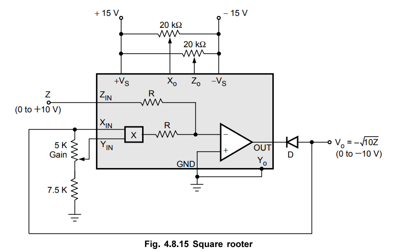
AD 533 as Square Rooter :
The
connection diagram of AD 533 as a square rooter is shown in the Fig. 4.8.15,
alongwith the component values. This mode is also a feedback configuration.
Both X and Y inputs are tied to the op-amp output through an external diode to
prevent latchup.
Accuracy,
noise and the frequency response are proportional to the √Z, which implies a
wider usable dynamic range than the divide mode.
The
output is given as,
Vo
= -√10Z
b.
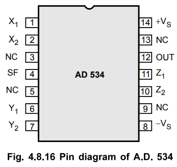
Study of Multiplier IC : AD 534
The
IC AD 534 is a multiplier IC by Analog Devices. It is a monolithic laser
trimmed four quadrant multiplier, having a maximum multiplication error of ±
0.25 %. It does not require any external trimming. It has excellent supply
rejection, low temperature coefficient and long term stability. It preserves
the accuracy even under adverse conditions of use.
It
is the first multiplier to offer fully the differential, high impedance
operation on all inputs, including the Z input. This has increased its
flexibility and simplicity of use.
The
scale factor is pretrimmed to the standard value of 10.00. By means of the
external resistor, the scale factor can be reduced to the values as low as 3,
with corresponding reductions in bias current and noise level. Its operating
temperature range is -55°C to+ 125°C.
The
AD 534 is the first general purpose multiplier, capable of providing gains upto
X100. It does not require the separate instrumentation amplifiers for
preconditioning of the inputs. The AD 534 can be very effectively employed as a
variable gain differential input amplifier with high Common Mode Rejection
Ratio (CMRR). The gain option is available in all the modes. It is very simple
to implement many function fitting algorithms as used to generate sine and
tangent, with AD 534. The utility of this feature is enhanced by the inherent
low noise of the AD 534 which is 90 |iV rms (depending on the gain). Drift and
feedthrough are also substantially reduced over earlier designs. The precise
calibration and differential Z input makes the AD 534 more flexible compared
to other multipliers. The standard MDSSR
(Multiplication, Division, Square and Square rooting) functions can be very
easily implemented using AD 534. The output can be in the form of a current if
required, facilitating the operations such as integration.
The
various features of AD 534 are
1)
Pretrimmed to ± 0.25 % maximum four quadrant error.
2)
All the inputs X,Y and Z are differential.
3)
The adjustable scale factor.
4)
Low noise design : 90 µV rms for 10 Hz -10 kHz
5)
Low cost monolithic construction
6)
Excellent long term stability
All
the grades of AD 534 are available in hermetically sealed TO-100 metal cans and
TO-116 ceramic DIP packages. The pin diagram of AD 534 is shown in the Fig.
4.8.16.
The
low cost and simplicity of operation of the AD 534 make it suitable for use in
the applications such as,
1)
Multiplier
2)
Divider
3)
Squarer and square rooter
4)
High quality analog signal processing
5)
Differential ratio and percentage computations
6)
Algebraic and Trignometric function synthesis
7)
Wideband and high crest rms to dc conversion
8)
Accurate voltage controlled oscillators and filters
Use
of AD 534 in some of the basic applications is discussed here.
1.
AD 534 as Divider
The
AD 534 as divider is shown in the Fig. 4.8.17.
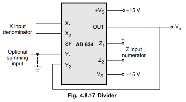
AD
534 provides the differential operation on both numerator and denominator. This
allows the ratio of two floating variables to be generated. Further flexibility
is possible from access to a high impedance summing input to Y1. The
bandwidth is proportional to the denominator magnitude.
Without additional trimming, the accuracy of AD 534 is sufficient to maintain a 1% error over 10 V to 1 V denominator range.
The
overall gain can be introduced by inserting a simple attenuator between the output
and Y2 terminal.
This
option and the differential ratio capability of AD 534 is utilised in the
percentage computer applications.
The
output of the AD 534 as a divider circuit, is
2. AD 534 as Square Rooter
The
square rooter circuit connections using AD 534 is shown in the Fig. 4.8.18.
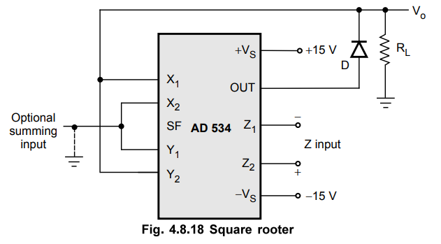
The
diode D prevents a latching condition which could occur if the input
momentarily changes the polarity. The output is always positive.
The
output can be changed to negative by reversing the diode direction and
interchanging the X inputs.
Since
the signal input is differential, all the combinations of input and output
polarities can be realized but operation is restricted to the one quadrant
associated with each combination of inputs.
The
output of the circuit is given as,
Vo = √10(Z2 – Z1) + X2
Review Questions
1. Draw the symbol of
analog multiplier IC and write expression for output voltage. List its
applications and explain any two.
May-07, Marks 8
2. With circuit
schematic explain how the multiplier IC AD533 can be used as squarer and
divider circuits.
Dec.-09, Marks 8
3. Write a note on
analog multipliers.
Dec.-08, 17, Marks 10
4. Explain how to
measure the phase difference between two signals.
Dec.-15, Marks 4
Linear Integrated Circuits: Unit IV: Special ICs : Tag: : Characteristics, Symbol, Block Diagram, Pin Diagram, Performance Parameters, Applications - Analog Multiplier IC
Related Topics
Related Subjects

Linear Integrated Circuits
EE3402 Lic Operational Amplifiers 4th Semester EEE Dept | 2021 Regulation | 4th Semester EEE Dept 2021 Regulation