Electron Devices and Circuits: Unit III: (a) BJT Amplifiers
Analysis of CE, CB and CC Amplifiers using re Model
BJT Amplifiers | Solved Example Problems
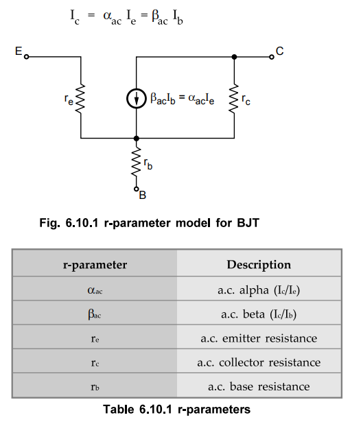
• The r-parameters (resistance -parameters) are perhaps easier to work with than h-parameters. Let us see the r-parameter model for transistor.
Analysis of CE, CB and CC Amplifiers using re Model
AU
: Dec.-18
•
The r-parameters (resistance -parameters) are perhaps easier to work with than
h-parameters. Let us see the r-parameter model for transistor. It is shown in
the Fig. 6.10.1. It consists of five r-parameters as listed in Table 1.4. The
rg is the ac emitter resistance, rc is the a.c. collector resistance and rb is
the a.c. base resistance. The current source is represented by
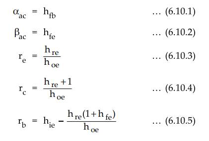
1. Relationships of r-Parameters and h-Parameters
•
Data sheets often specify the common emitter h-parameters of the transistor. In
such situations, we have to convert these parameters into r-parameters to
analyze transistor amplifier using r-parameters. The conversion formulae are as
follows :
2. Simplified r-Parameter Model for BJT
•
In a forward biased condition of base-emitter junction rb is very small and its
effect is also small enough to neglect it. Thus it can be replaced by a short
circuit. The collector-base junction is always reverse biased in the active
region. In this biasing state, a.c. collector resistance rc is usually several
hundred kilo-ohms, and hence it can be replaced by an open circuit. This gives
the simplified r-parameter model for BJT as shown in the Fig. 6.10.2.

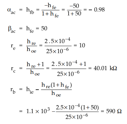
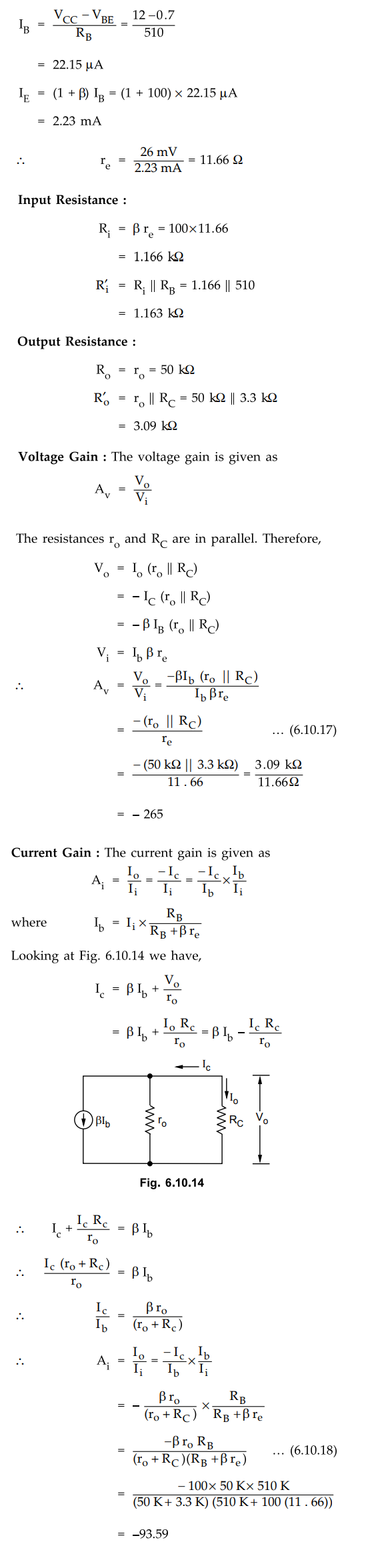
Ex.
6.10.1 Determine the r-parameters of a transistor if the h-parameters are hie =
1.1 k Ω hfe = 50, hoe = 25 µA/V and hre = 2.5
× 10-4
Sol.
:
Referring Table 6.10.1 and equation (6.10.1) through equation (6.10.5) we have,
3. r-Parameter Model for CB Configuration
•
The simplified r-parameter shown in the Fig. 6.10.3 is nothing but the
r-parameter model for common base configuration. However, in this section we
are going see the determination of r-parameter model for common base
configuration in a different way.
•
The re model employs a diode and controlled current source to duplicate the
behaviour of a transistor in the active region. The Fig. 6.10.3 shows the
common base transistor configuration and its rg model. The forward biased base
emitter junction in the active region is replaced by the PN junction diode. The
forward biased base emitter junction causes collector current to flow which
intum depends upon the base current. This input, output current relationship is
represented by a controlled current source whose value is

•
We know that, a.c. resistance of diode can be determined by the equation
rac
= 26mV / ID … (6.10.6)
where
ID is the d.c. current through the diode at the Q point. This same
equation can be used to find the a.c. resistance of the diode in Fig. 6.10.3
(b). If we substitute diode current equal to IE we get
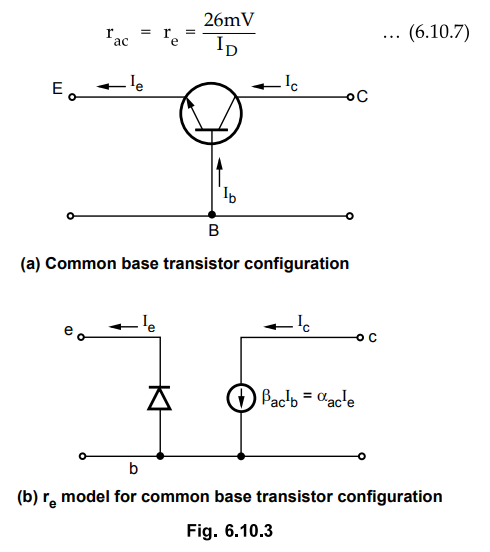
•
The subscript e or rg is chosen to emphasize that it is the d.c. level of
emitter current that determines the a.c. resistance of the diode in the Fig.
6.10.3 (b). Replacing the diode by its equivalent resistance we get the
r-parameter model for circuit, as shown in the Fig. 6.10.3.
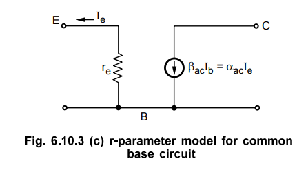
• Input Resistance :
Due to the isolation that exists between input and output circuit of Fig.
6.10.3, it is fairly obvious that the input resistance for the common base
configuration of a transistor is simply re . That is
R1
= re ... (6.10.8)
•
The typical value of R;, for common base configuration range from a few ohms to
a maximum of about 50 Ω .
Output
Resistance : To determine the output resistance we
have to make signal zero i.e. Ie = 0. When Ie = 0, ɑ Ie
is also zero and output is open-circuited. Therefore,
Ro
= ∞ ... (6.10.9)
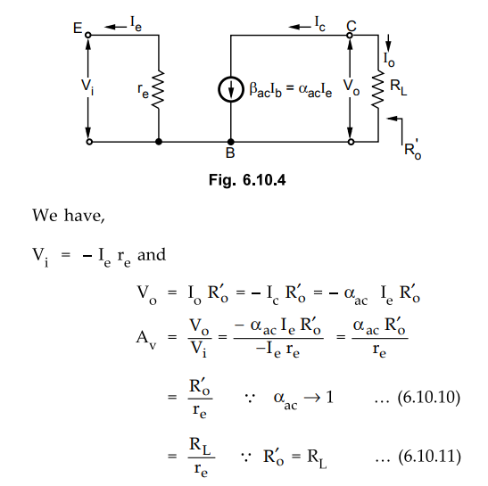
Voltage
Gain : The voltage gain is given as
AV
= Vo / Vi
•
It can be determined considering the load connected at the output terminals as
shown in the Fig. 6.10.4.
•
Looking at Fig. 6.10.4,
Current
Gain : The current gain is given as
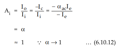
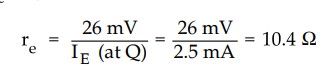
Ex.
6.10.2 Determine the value of re when d.c. emitter current at
operating point is 2.5 mA.
Sol.
:
The re is given as
Ex.
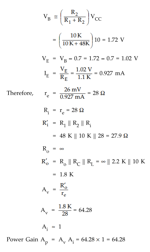
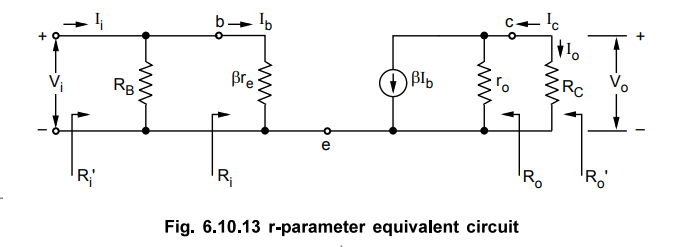
6.10.3 Determine the If, Ri, A^ A? R° and power gain for the common base
amplifier shown in Fig. 6.10.5.
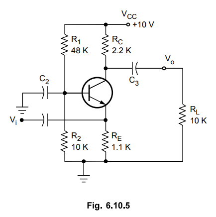
Sol.
:
The
r-parameter equivalent circuit for a given amplifier is shown in Fig. 6.10.6.
It is drawn by short circuiting d.c. source and all capacitors, and replacing
transistor by its r-parameter model.
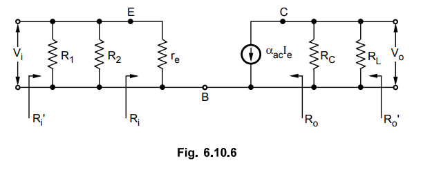
To
determine rg we have to first find IE. It is calculated as follows :
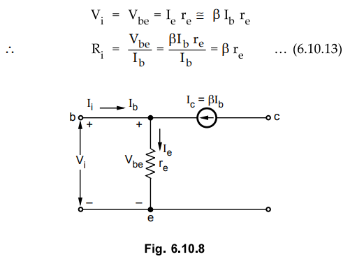
4. r-Parameter Model for CE Configuration
•
We know, for common emitter configuration, the input terminals are the base and
the emitter and output terminals are collector and emitter. The Fig. 6.10.7
shows the common emitter configuration and its rg model. Here, also the rg
model employs a diode and controlled current source to duplicate the behaviour
of a transistor in the active region. The forward biased base emitter junction
in the active region is represented by the diode and controlled current source
is still connected between the collector and the base terminals.
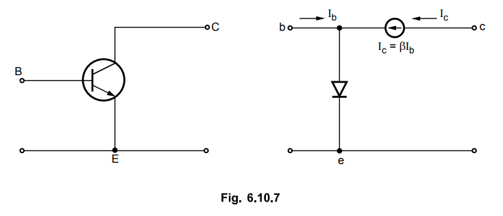
•
Looking at the model we have current through diode equal to
•
The input resistance is given by
•
The voltage Vbe is across the diode resistance as shown in Fig. 6.10.8. The
level of rg is still determined by the d.c. current I£. Using Ohm's law gives
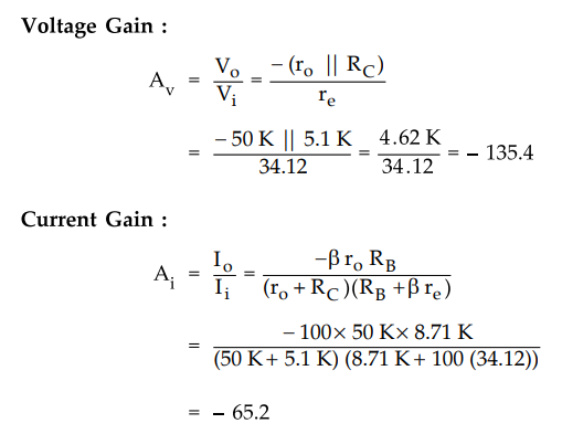
• The typical value of Riz for common emitter configuration range from a few hundred ohms to maximum about 6-7 kilo ohms.
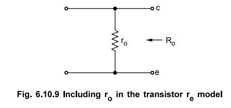
• Output resistance : The rg model in Fig. 6.10.9 does not include an output resistance. However, if it is available from a graphical analysis or from data sheets it can be included as shown in Fig. 6.10.9.
•
When input is short circuited, Ib = 0 and I = 0 and output resistance is given
as
Ro
= ro ... (6.10.14)
•
If ro is ignored from re model of CE, the output
resistance is ∞
Voltage
Gain : The voltage gain is given as
Av
= Vo / Vi
•
It can be determined considering the load connected at the output terminals and
output resistance as shown in Fig. 6.10.10.
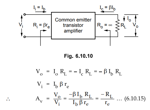
•
The negative sign in the resulting equation for indicates that a 180 ° phase
shift occurs between the input and output signals.
Current
Gain : The current gain is given as
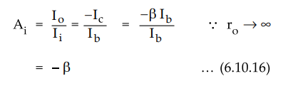
•
Using the derived values of input resistance (P rg), the collector current (P
Ib), and the output resistance (rQ), the equivalent model for common emitter
configuration can be given as shown in the Fig. 6.10.11.
a.
Analysis of Common Emitter Fixed Bias Configuration
•
Let us consider a common emitter amplifier with a bias, as shown in Fig. 6.10.12.

•
By short-circuiting C1, C2 and dc power supply, and
replacing transistor with its equivalent r-parameter model (Refer Fig. 6.10.11)
we get the r-parameter equivalent circuit for given transistor amplifier as
shown in Fig. 6.10.11.
•
To find the rg we have to first determine the IE. It can be calculated as
follows :
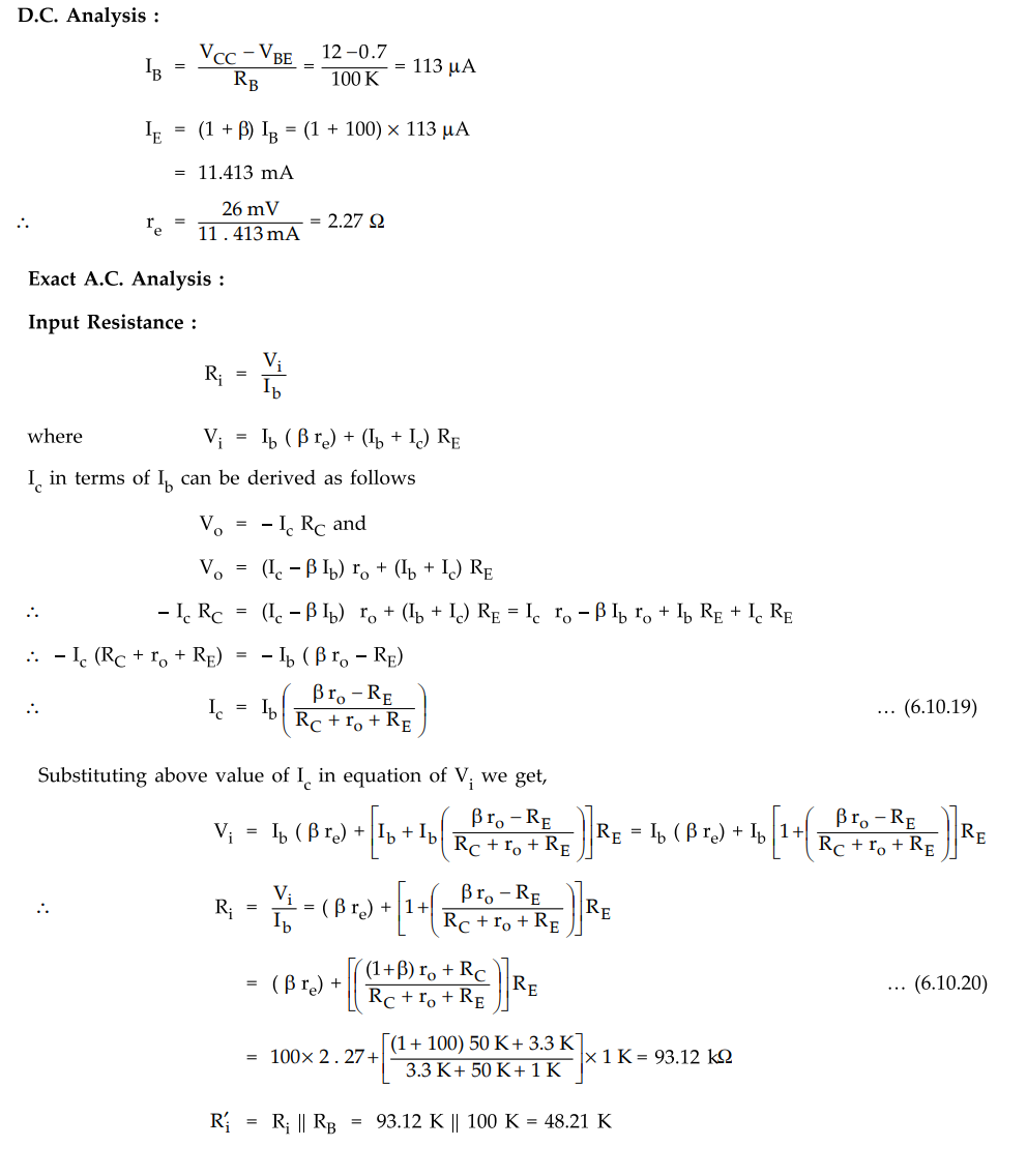
D.C.
Analysis :
b.
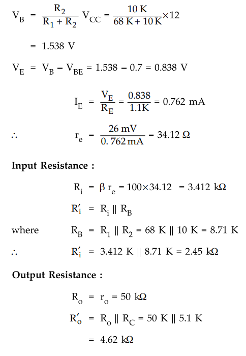
Analysis of Common Emitter Voltage Divider Bias Configuration
•
Let us consider a common emitter amplifier with a voltage divider bias, as
shown in Fig. 6.10.15.
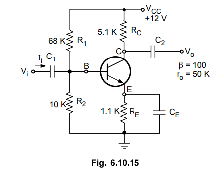
•
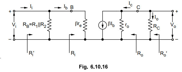
By short circuiting C1, C2, CE and d.c. power
supply, and replacing transistor with its equivalent r-parameter model we get
the r-parameter equivalent circuit for given transistor amplifier, as shown in
Fig. 6.10.16.
•
To find the re we have to first determine the IE. It can be calculated as
follows :
•
D.C. Analysis : If β RE > 10 R2 we can use approximate
approach.
100
× 11 K > 10 × 10 K
110
K > 100 K
Using
the approximate approach we have,
The
equivalent circuit shown in Fig. 6.10.16 and Fig. 6.10.13 are same. Thus by
using same analysis we have,
Voltage
Gain :
Ex.
6.10.4 For the circuit shown below, find i) d.c. bias levels ii) d.c. voltages
across the capacitors iii) a.c. emitter resistance iv) voltage gain and v)
state of the transistor.

Sol.
: i) DC bias levels
DC
voltage across R2 (V2)
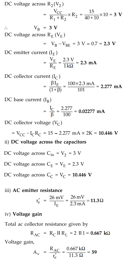
v)
State of the transistor
As
calculated, VC = 10.446 V and VE = 2.3 V
Since
VC >VE, the transistor is in active state.
c.
Analysis of Common Emitter with Unbypassed RE
•
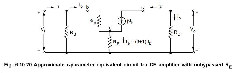
Let us consider a common emitter amplifier with unbypassed RE, as shown in Fig.
6.10.18.
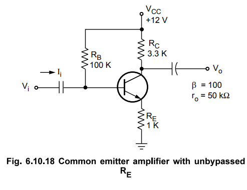
•
By short-circuiting C1, C1 and d.c. power supply, and
replacing transistor with its equivalent r-parameter model we get the
r-parameter equivalent circuit for given transistor amplifier, as shown in Fig.
6.10.19.
D.C.
Analysis :
Output
Resistance : With Vi set to zero, Ib
= 0, β Ib = 0 and (1 + β) Ib = 0, and can be replaced by
open circuit.
Ro
= RC
=
3.3 kΩ ... (6.10.21)
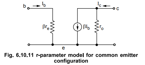
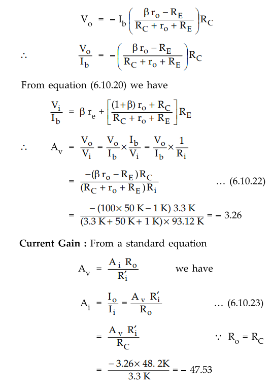
Voltage
Gain : AV = Vo / Vi
where
Substituting
value of Ic from equation (6.10.19) we get
Approximate
A.C. Analysis :
•
The Fig. 6.10.20 shows the approximate r-parameter equivalent circuit for
common emitter amplifier with unbypassed RE, In the approximate A.C. analysis
we have assumed ro = ∞
Input
Resistance :
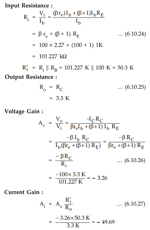
Note
:
The analysis approach (Exact or approximate) can be selected by testing
following two conditions :
1.
ro ≥ 10 (RC + RE) and 2. ro ≥ 10 RC
If
both the conditions are satisfied we can use approximate approach.
d.
Analysis of Common Emitter with Collector Feedback Configuration
•
Let us consider a common emitter amplifier with a collector feedback
configuration, as shown in the Fig. 6.10.21.
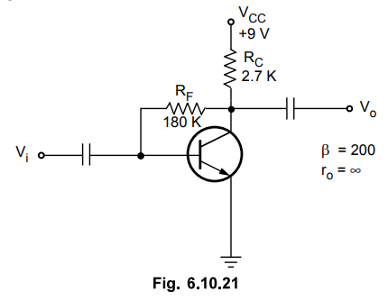
•
Applying Miller's theorem (Refer section 6.7.1) we have,
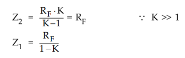
•
Therefore, the r-parameter equivalent circuit for given amplifier circuit is as
shown in the Fig. 6.10.22.
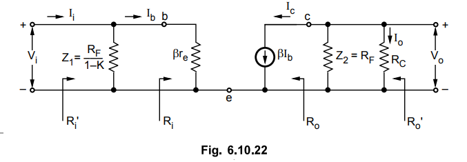
D.C.
Analysis :
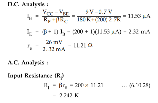
Output Resistance
When
Vi = 0, Ib = 0 and β Ib = 0 and they can be
treated as open circuit.
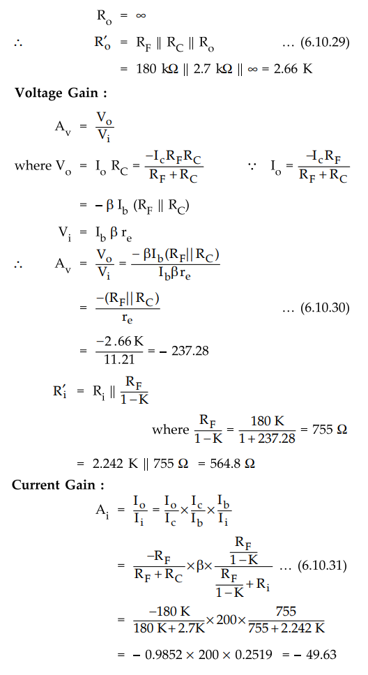
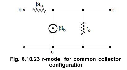
5. r-Parameter Model for CC Configuration
•
For the common collector configuration the model defined for the common emitter
configuration with unbypassed RE is applied rather than defining a model for
the common collector configuration. In common collector configuration the
output is taken from the emitter terminal. Thus resistance Pre appears between
input and output, and the direction of current source gets exactly reverse to maintain
current flow from collector to emitter. The Fig. 6.10.23 shows the modified
model of common-emitter configuration which can be used to analyse common
collector amplifier.
•
Let us consider a common collector amplifier as shown in the Fig. 6.10.24.
•
By short circuiting Clz C2 and d.c. power supply, and replacing transistor with
its equivalent r-parameter model we get the r-parameter equivalent circuit for
given transistor amplifier, as shown in the Fig. 6.10.25.
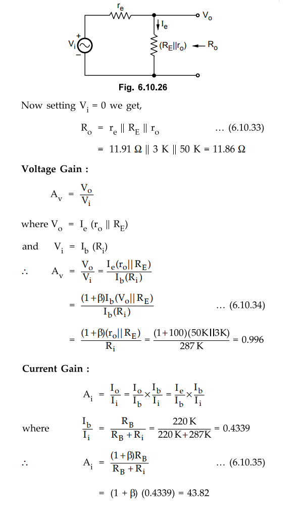
D.C.
Analysis :
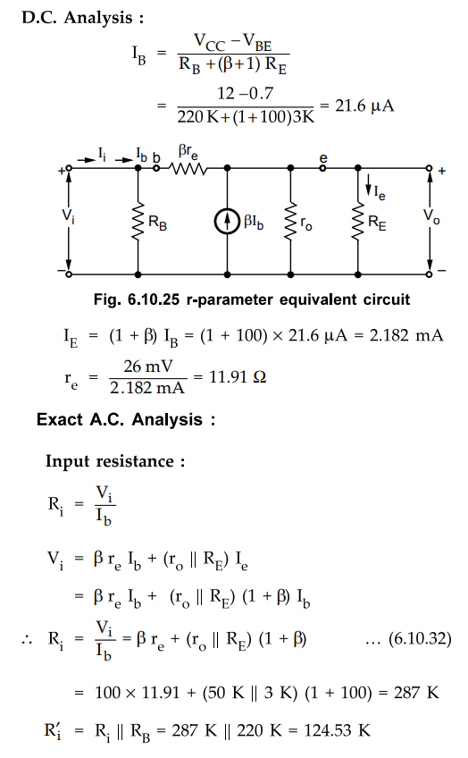
Output
Resistance :
•
When Vi is set to zero, Ife becomes theoretically zero which
eventually makes Ie zero. Students may get confused while calculating R o
due to this theoretical aspect.
•
Practically, in this case it is necessary to consider the effect of Ife at the
output side, while calculating R o. This can be mathematically
expressed as,
We
know that
I
b = Vi / R i
The
Ib can be expressed interms of Ie as,
Ie
= (β + 1) Ib = (β + 1) Vi / Ri
Substituting
Ri in above equation we get,
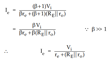
The
relationship of Ie and Vi given by above equation can be represented by network
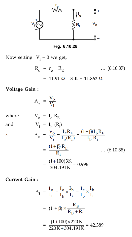
shown in the Fig. 6.10.26
Approximate
A.C. Analysis
•
The Fig. 6.10.27 shows the approximate r-parameter equivalent circuit for
common collector amplifier. In the approximate A.C. analysis we have assumed ro
= ∞

The
relationship of Ie and Vi given by above equation can be represented by network
shown in the Fig. 6.10.28
Review Questions
1. Explain the rg transistor model.
2. Give the relationship between r-parameter and h-parameters.
Electron Devices and Circuits: Unit III: (a) BJT Amplifiers : Tag: : BJT Amplifiers | Solved Example Problems - Analysis of CE, CB and CC Amplifiers using re Model
Related Topics
Related Subjects

Electron Devices and Circuits
EC3301 3rd Semester EEE Dept | 2021 Regulation | 3rd Semester EEE Dept 2021 Regulation