Electron Devices and Circuits: Unit III: (a) BJT Amplifiers
Analysis of CE Amplifier with Collector to Base Bias
Miller’s Theorem, Solved Example Problems | BJT Amplifiers
• For the analysis of this circuit it is necessary to split this resistance for input and output. This can be achived by using Miller’s theorem.
Analysis of CE Amplifier with Collector to Base Bias
•
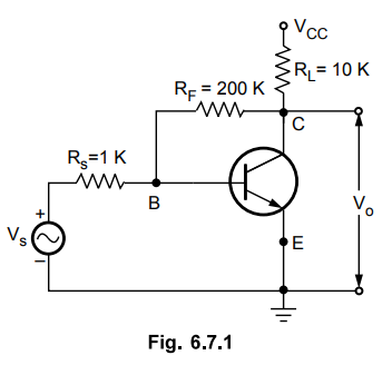
The Fig. 6.7.1 shows the common emitter amplifier with collector to base bias.
•
As shown in the Fig. 6.7.1, the resistance RF in this configuration is
connected between input and output.
•
For the analysis of this circuit it is necessary to split this resistance for
input and output. This can be achived by using Miller’s theorem.
1. Miller’s Theorem
•
In general, the Miller theorem is used for converting any circuit having
configuration of Fig. 6.7.2 (a) to another configuration shown in Fig. 6.7.2
(b).
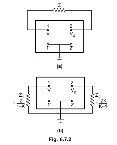
• The Fig. 6.7.2 shows that, if Z is the impedance connected between two nodes, node 1 and node 2, it can be replaced by two separate impedances Z1 and Z2; where Z1 is connected between node 1 and ground and Z2 is connected between node 2 and ground.
•
The Vi and Vo are the voltages at the node 1 and node 2 respectively. The
values of Z1 andZ2 can be derived from the ratio of Vo and V; (Vo / Vi),
denoted as K. Thus it is not necessary to know the values of V; and Vo to calculate
the values of Zi and Z2.
•
The values of impedances Z1 and Z2 are given as Z
Z1 = Z / 1 – K … (6.7.1)
And
Z2 = Z.K / K – 1 … (6.7.2)
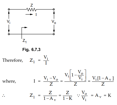
2. Proof of Miller's Theorem
Miller's
theorem states that, the effect of resistance Z on the input circuit is a ratio
of input voltage V to the current I which flows from the input to the output.
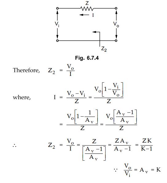
•
Miller's theorem states that, the effect of resistance Z on the output circuit
is a ratio of output voltage Vo to the current I which flows from the output to
the input.
3. Analysis using Miller's Theorem
• For the common emitter amplifier with
collector to base bias shown in Fig. 6.7.5, calculate Ri, Ai ,
Av Avs and Ro. The transistor parameters are hie = 1.1 K,
hfe = 50, hoe = hre = 0 . Assume RL
= 10 K and Rs = 1 K
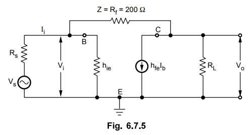
H-parameter
equivalent circuit :
•
The Fig. 6.7.5 shows the approximate h-parameter equivalent circuit for the
amplifier shown in Fig. 6.7.1.
•
Applying Miller's theorem we get simplified circuit as shown in the Fig. 6.7.6.
The voltage Av of the circuit can be given as Vo / Vi. AS the amplifier is a common
emitter amplifier we can assume that the voltage gain Av >> f i.e. K
>> 1. This assumption makes it easier to calculate the value of Z2.
Z2 is given as,
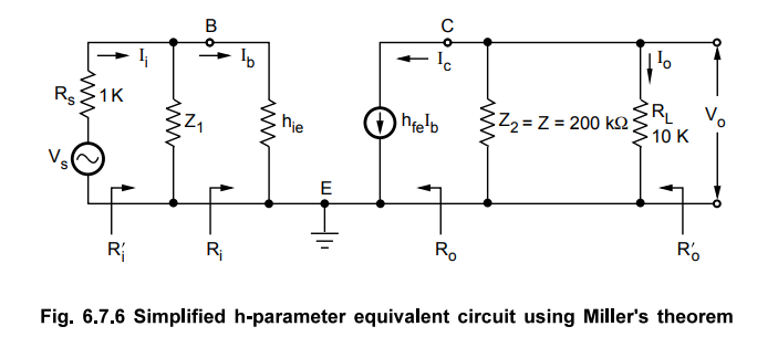
Z2
= Z • K / K – 1 = Z • K / K K >>
1
Z2
= Z = 200 kΩ
However,
we do not know the exact value of Av, thus we cannot calculate exact value of
Z1 at this stage.
Analysis
:
Since
h oe = h re = 0, we use approximate analysis
a)
Current gain ( Ai ) = - hfe = - 0
b)
Input resistance ( Ri ) = hie = 1.1 kΩ
c)
Voltage gain (Av) = Ai RL / Ri

Ex.
6.7.1 The transistor used in the circuit of Fig. 6.7.9 has following
parameters, hfe = 500 Ω,
hre
= 2.4 × 10- 4, hfe = 60 and hoe = 1/40 K.
Calculate Rv, Ri ,
AI , AV , AVe = AVe = Vo /
Vs , AI = IL / Is and R'o. Assume all capacitors to
be very large.
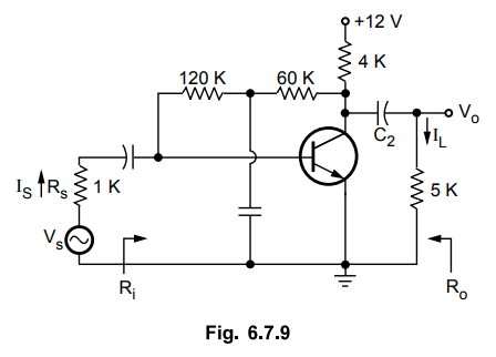
Sol.
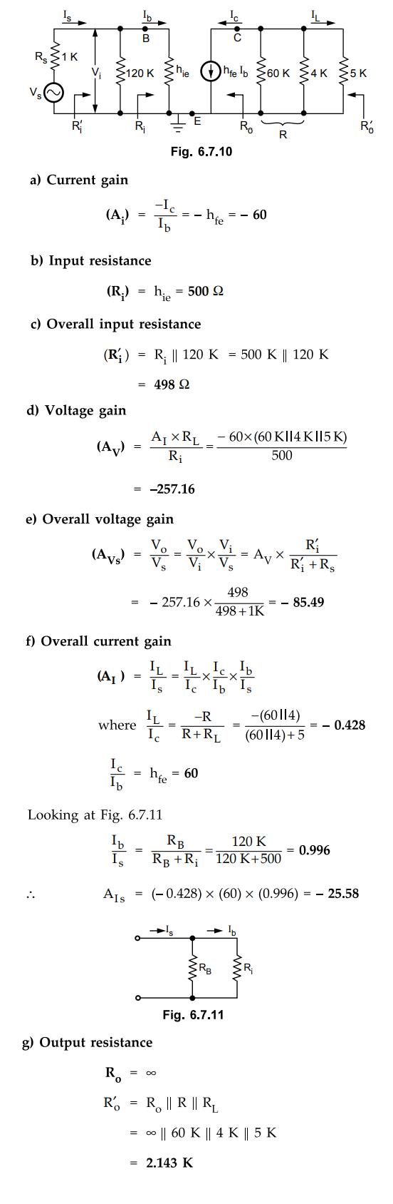
: For the given circuit hoe × R'L where
R'L=(RL
||R) = 1 / 40 × 103 × (60K||4K|| 5K) = 0.0536,
which
is less than 0.1. Thus we analyze given circuit with approximate method. Fig.
6.7.10 shows approximate h-parameter equivalent circuit for given circuit. It
is drawn by replacing all capacitors and d.c. source with short circuits and
replacing transistor with its h-parameter equivalent circuit.
Review Question
1. Define Miller's theorem.
Electron Devices and Circuits: Unit III: (a) BJT Amplifiers : Tag: : Miller’s Theorem, Solved Example Problems | BJT Amplifiers - Analysis of CE Amplifier with Collector to Base Bias
Related Topics
Related Subjects

Electron Devices and Circuits
EC3301 3rd Semester EEE Dept | 2021 Regulation | 3rd Semester EEE Dept 2021 Regulation