Electron Devices and Circuits: Unit III: (b) MOSFET Amplifier
Analysis of Common-Source (CS) Amplifier
Equivalent circuit, Solved Example Problems | MOSFET Amplifier
• In this section, we will see the common-source amplifier. We will analyze several basic common-source circuits and will determine small-signal voltage gain and input and output impedances.
Analysis of Common-Source (CS) Amplifier
•
In this section, we will see the common-source amplifier. We will analyze
several basic common-source circuits and will determine small-signal voltage
gain and input and output impedances.
1. Basic Common-Source Configuration
•
The Fig. 7.4.1 shows the common source circuit with voltage divider biasing and
coupling capacitor. The MOSFET is biased near the middle of the saturation
region by R1 and R2 resistors to work as an amplifier.

•
Assume that, the signal frequency is sufficiently large for the coupling
capacitor to act essentially as a short circuit. The signal source is
represented by a Thevenin equivalent circuit, in which the signal voltage
source vs, is in series with an equivalent source resistance Rsi.
•
Here Rsi should be much less than the amplifier input resistance, Ri
= R1 || R2 in order to minimize loading effects.
•
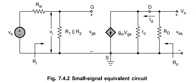
Fig. 7.4.2 shows the resulting small-signal equivalent circuit.

•
The input gate-to-source voltage is

•
So the small-signal overall voltage gain is,

•
Since Rsi is not zero, the amplifier input signal v4 is less than the signal
voltage. This is known as loading effect. It reduces the voltage gain of the
amplifier.
•
The input resistance is Ris = R1 || R2
•
The output resistance is Ro = RD || ro
•
We can also relate the a.c. drain current to the a.c. drain-to-source voltage,
as
Vds
= - Id(RD).
•
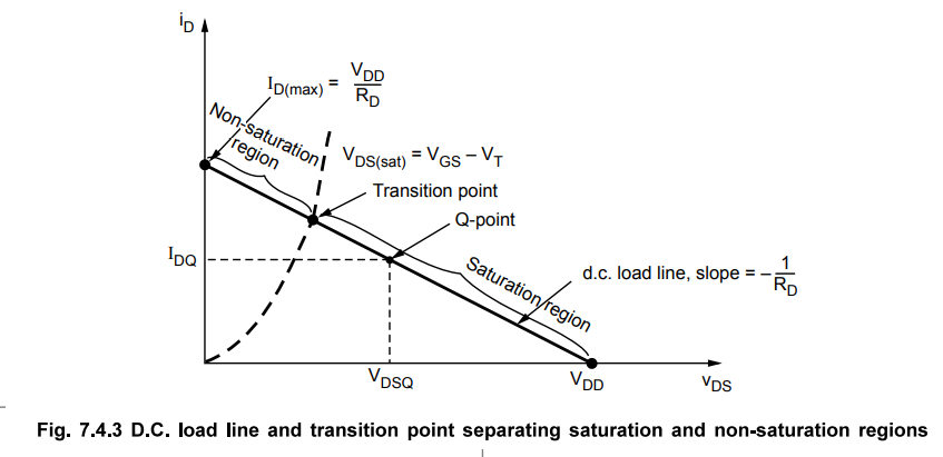
Fig. 7.4.3 shows the d.c. load line, the transition point, and the Q-point,
which is in the saturation region.
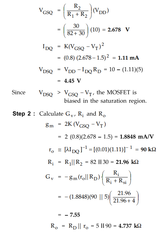
Ex.
7.4.1 For the circuit shown in Fig. 7.4.4, the MOSFET parameters are : VT = 1.5
V, = OB mA/V2 and λ = 0.01 V-1, determine the small
signal voltage gain, Ri ,
and Ro.

Sol.
:
Step
1 :
D.C. analysis : The d.c. or quiescent gate-to-source voltage is,
Ex.
7.4.2 Describe the small-signal voltage gain, input and output resistance of a
common source amplifier. For the circuit shown below in Fig. 7.4.5 the parameters
are VDD=10 V, = 70.9 kΩ, R2 = 29.1 kΩ, RD = 10 kQand RL =10kΩ. The
transistor parameters are Vm = 1.5 V, Kn = 0.5 mA/v2 and X =0.01
V-1,

Sol
.:
Step 1 : D.C. Analysis
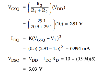
Since
VDSQ > VGSQ – VT, The MOSFET is biased in the saturation region.
Step
2 : A.C. Analysis

Ex.
7.4.3 A common source amplifier using EMOSFET is shown in Fig. 7.4.6. Assume
for this device I DON) = 200 mA at VGS(ON) = 4 V. VT = 2 V and gm = 23 mS, Vin
= 25 mV
i)
VGS ii) ID iii) VDS iv) a.c. output voltage.
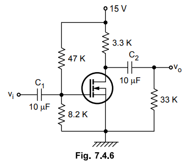
Sol. :
Step
1 : Calculate VGS, IDQ, VDS

2. Common-Source Amplifier with Source Resistor
•
Fig. 7.4.7 shows the common source amplifier with source resistor.
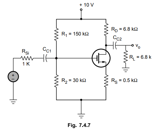
•
The source resistor is introduced to stabilize the Q-point against variations
in the MOSFET parameters. However, like in BJT circuits, a source resistor reduces
the signal gain.
Ex.
7.4.4 Consider the circuit in Fig. 7.4.7. The MOSFET parameters are VT
= 0.8 V. K= 1 mA/V2, and 7=0. Calculate the voltage gain of the amplifier.
Sol.
:
Step
1 : DC analysis
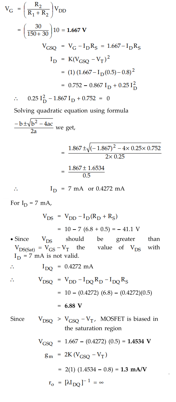
Step
2 :
Draw the small signal equivalent circuit Fig. 7.4.8 shows the small signal
equivalent circuit, for the common source amplifier circuit with source
resistor.

3. Common-Source Circuit with Source Bypass Capacitor
•
A source bypass capacitor connected across the source resistor in the
common-source circuit will minimize the loss in the small signal voltage gain,
while maintaining Q-point stability.
•
The Q-point stability can be further increased by replacing the source resistor
with a constant-current source.
•
The Fig. 7.4.9 shows common source circuit with source bypass capacitor. It
acts as short circuit for a.c. signal and open circuit for d.c. signal.

Ex.
7.4.5 For the circuit shown in Fig. 7.4.9, the MOSFET parameters are : VT
= 0.8 V, K = tmA/V2, and λ = 0. Calculate the voltage gain.
Sol.
:
Step
1:
DC analysis
Since
the d.c. gate current is zero, the d.c. voltage at the source terminal is Vs
=- VGSQ, and the gate-to-source voltage is determined from

The
quiescent drain-to-source voltage is

Since
VDS > Vgs - VT = 1.51 - 0.8 = 0.71 V,
transistor is biased in the saturation region.
Step
2:
Draw the small signal equivalent circuit.
gm
= 2K (VGS -VT) (VGS-VT)
=
2(1) (1.51 0.8)
=
1.42 mA/V
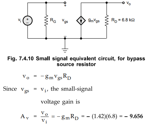
Important Concept
Comparing
the small signal voltage gain of - 9.656 in this example to the - 5.36
calculated in example 7.4.4, we see that the magnitude of the gain increases
when a source bypass capacitor is included.
Ex.
7.4.6 For the common source amplifier circuit shown in Fig. 7.4.11.
Determine
:
i)
gm ii) Av iii) Ri Ri
iv) Avs v) Ro and R'o
Given
:
K
= 04 mA/V2, VT = 3 V, ID =111 mA VGS
= 466 V, ro = 40 k Ω

Review Questions
1. Draw and explain the common source amplifier with source
resistor.
2. Draw and explain the common source amplifier with bypassed
source resistor.
3. With neat circuit diagram, perform ac analysis for common
source using equivalent circuit NMOSFET amplifier.
Electron Devices and Circuits: Unit III: (b) MOSFET Amplifier : Tag: : Equivalent circuit, Solved Example Problems | MOSFET Amplifier - Analysis of Common-Source (CS) Amplifier
Related Topics
Related Subjects

Electron Devices and Circuits
EC3301 3rd Semester EEE Dept | 2021 Regulation | 3rd Semester EEE Dept 2021 Regulation