Electron Devices and Circuits: Unit V: (a) Feedback Amplifiers
Analysis of Feedback Amplifiers
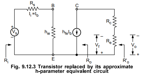
• Fig. 9.12.1 shows the transistor emitter follows circuit. Here, feedback voltage is the voltage across Ro and sampled signal is Vo across Re.
Analysis of Feedback Amplifiers
AU
: May-06, 07, 10, 11, 12, 13, 15, 16, Dec.-05, 08, 10, 14, 15
1. Voltage Series Feedback
•
Fig. 9.12.1 shows the transistor emitter follows circuit. Here, feedback voltage
is the voltage across Ro and sampled signal is Vo across Re.

Analysis
Step
1 :
Identify topology
• By shorting output voltage (Vo = 0), feedback signal becomes zero and hence it is voltage sampling. Looking at Fig. 9.12.1 we can see that feedback signal Vf is subtracted from the externally applied signal Vs and hence it is a series mixing. Combining two conclusions we can say that it is a voltage series feedback amplifier.
Step
2 and Step 3 : Find input and output circuit
•
To find the input circuit, set Vo = 0, and hence Vs in series with Rs appears
between B and E. To find the output circuit, set Ii = Ib = 0, and hence Re
appears only in the output loop. With these connections we obtain the circuit
as shown in the Fig. 9.12.2

Step
4 :
Replace transistor by its h-parameter equivalent circuit
Step
5 :
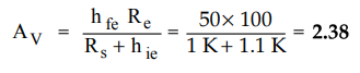
Find open loop voltage gain
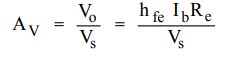
Applying
KVL to input loop we get
Vs
= Ib (Rs + hie)
Substituting
value of Vs we get
Step
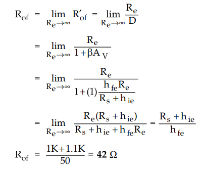
6 : Indicate Vo and Vf and calculate β

•
The output resistance is measured by making
Vs
= 0. Since Vs = 0, Ib = 0 and hence hfeIb = 0, as shown in the Fig. 9.12.4.

•
The indeterminancy Rof = ∞ may resolved by deriving Rof
interms of Rof.
a.
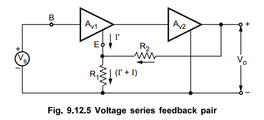
Voltage Series Feedback Pair
•
Fig. 9.12.5 shows two cascaded stages. The output of second stage is connected
through feedback network to the input of first stage in opposition to the input
signal Vs.
Analysis
:
Step
1 :
Identify topology
•
By shorting output voltage Vo = 0, feedback signal becomes zero and
hence it is voltage sampling. Looking at Fig. 9.12.5 we can see that feedback
signal Vf is subtracted from the externally applied signal Vs and hence it is a
series mixing. Combining two conclusions we can say that it is a voltage series
feedback amplifier.
Step
2 and Step 3 : Find input and output circuit
•
To find input circuit, set Vo = 0 in Fig. 9.12.5 and hence R2 appears m
parallel with Rj at first emitter. To find the output circuit, set Ii = 0 in
Fig. 9.12.5 and hence T = 0 (open circuit) and Rj appears in series with R2
across output. The resulting circuit is shown in Fig. 9.12.6.

For
this circuit, feedback factor β can be calculated as
β
= Vf / Vo = R1 / R1 + R2
Ex.
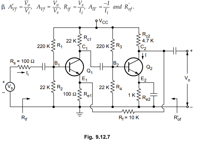
9.12.1 Transistors in the feedback amplifier shown in Fig. 9.12.7 are identical
and their 'h' parameters are hie =1100 Ω hf= 50, hre = hoe= 0. Neglect
capacitances of all capacitors.
i)
State topology with justification, ii) Calculate
Sol
: Step 1 : Identify topology
The
feedback voltage is applied across the resistance Re1 and it is in series with
input signal. Hence feedback is voltage series feedback.
Step
2 and Step 3 : Find input and output circuit
To
find input circuit, set Vo = 0 (connecting C2 to ground), which gives parallel
combination of Re with Rf at Ep To find output circuit, set Ii = 0 (opening the
input node E1 at emitter of Q1), which gives series combination of Rf and Re1
across the output. The resultant circuit is shown in Fig. 9.12.8.

Step
4 :
Replace transistors with hybrid equivalent circuit.

Ex.
9.12.2 Find the voltage gain, feedback factor, input resistance and output
resistance of a series-shunt pair type two stage feedback amplifier using
transistors with hfe = 99 and hig = 2 k Ω,
shown in Fig. 9.12.10.

Sol.
: Step 1 : Identify topology
The
feedback voltage is applied across the resistance R4 and it is in series with
input signal. Hence feedback is voltage series feedback.
Step
2 and Step 3 : Find input and output circuit. To find input circuit, set V = 0,
which gives parallel combination of R4 with R3 at Ej. To find output circuit,
set Ij = 0, which gives series combination of R3 and R4 across the output. The
resultant circuit is shown in the Fig. 9.12.11.
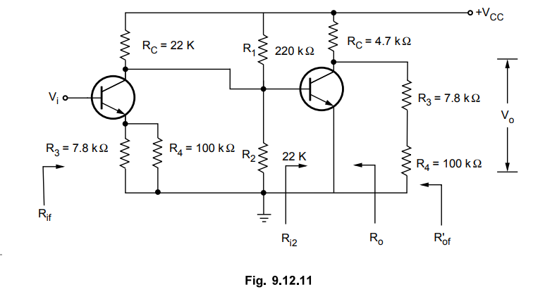
Step
4 : Find open loop voltage gain (AV)

Ex.
9.12.3 For feedback amplifier shown in Fig. 9.12.13, identify the feedback
topology with proper justification. The transistors used are identical with the
following parameters :

Sol.
: Step 1 : Identify topology.
The
feedback voltage is applied across Rgl = 1.5 K, which is in series with input
signal. Hence feedback is voltage series feedback.
Step
2 and Step 3 : Find input and output circuit To find
input circuit, set VQ = 0, which gives parallel combination of Rgl with Rf at
Ej as shown in the Fig. 9.12.14. To find output circuit, set L = 0 by opening
the input node, Ej at emitter of Qj, which gives the series combination of Rf
and Rgl across the output. The resultant circuit is shown in Fig. 9.12.14.

Step
4 :
Find the open loop voltage gain (AV).

Example
for Practice
Ex.
9.12.4 Transistors in the feedback amplifier shown in Fig. 9.12.16 are
identical and transistor parameters are hle = 1.1 K, h^, = 50, hre = = 0. Identify the feedback amplifier and
calculate Avf, R'of and Rlf.
AU
: ECE : Dec.-lO, Marks 16
[Ans.:
Voltage series feedback amplifier, Avf = 45.46, Ro =112 k Ω,
Rif = 27.12 kQ, Rof = 129 Ω]

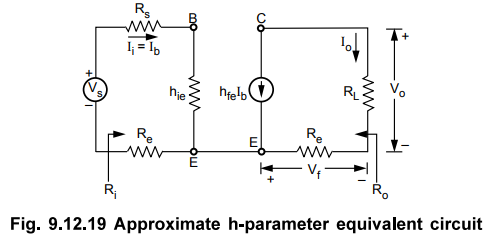
2. Current Series Feedback
•
Fig. 9.12.17 shows the common emitter circuit with imbypassed Rg. The common
emitter circuit with unbypassed Rg is an example of current series feedback. In
this configuration resistor Re is common to base to emitter input circuit as
well as collector to emitter output circuit and input current Ib as well as
output current Ic both flow through it. The voltage drop across RE

•
Vf = (Ib + Ic) Re = Ie Re ≈ R Re = Io R Re’
This voltage droP shows that the output current I is being sampled and it is
converted to voltage by feedback network. At input side voltage Vf is
subtracted from Vg to produce V.. Therefore, the feedback applied in series.
Analysis
Step
1 :
Identify topology
•
By opening the output loop, (output current, Io = 0), feedback signal becomes
zero and hence it is current sampling. Looking at Fig. 9.12.17 we can see that
feedback signal Vf is subtracted from the externally applied signal V hence it
is a series mixing. Combining two conclusions we can say that it is a current
series feedback amplifier.
Step
2 and Step 3 : Find input and output circuit
•
To find input circuit set Io = 0, then R appears at the input side. To find
output circuit set I; = 0, then Re appears in the output circuit. The resulting
circuit is shown in the Fig. 9.12.18.

Step
4 :
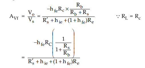
Replace transistor with its approximate h-parameter equivalent circuit
•
Fig. 9.12.19 shows the approximate h-parameter equivalent circuit
Step 5 : Find open loop
transfer gain

Ex.
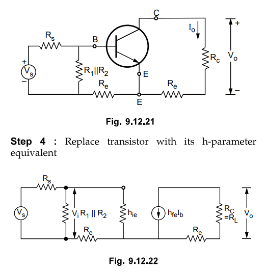
9.12.5 For the circuit shown in Fig. 9.12.20. i) Identify topology used in
feedback amplifier ii) Show that voltage gain with feedback

Sol.
:
Step
1 :
Identify topology
By
shorting output (V = 0), feedback voltage does not become zero. By opening the
output loop feedback becomes zero and hence it is current sampling. The
feedback is applied in series with the input signal, hence topology used is
current series feedback.
Step
2 and Step 3 : Find input and output circuit To find
input circuit, set I = 0. This places Rg in series with input. To find output
circuit L = 0. This places Rg in the output side. The resultant circuit is
shown in Fig. 9.12.21.
Step
5 :
Find open loop transfer gain
Referring
expressions of GM, D and P from previous example we have,

Dividing
both numerator and denominator by Rs + Rb
we
get
Ex.
9.12.6 A current series feedback amplifier is shown in the Fig. 9.12.23 below.
It
has the following parameters :

Sol.
:
The Fig. 9.12.24 shows the equivalent circuit for the given current series
feedback amplifier.

3. Current Shunt Feedback
•
Fig. 9.12.25 shows two transistors in cascade connection with feedback from
second emitter to first base through resistor R'. Here, the feedback network
formed by R' and Re2 divides the current Ig. Since I = - 1^ the feedback
network gives current feedback. At input side, we see that I; = Is - If, i.e.
If is shunt subtracted from Ig to get If Therefore, this configuration is a
current shunt feedback.
Step
1 :
Identify topology
•
By shorting output voltage (V = 0), feedback signal does not become zero and
hence it is not voltage sampling. By opening the output loop (Io = 0), feedback
signal becomes zero and hence it is a current feedback. The feedback signal
appears in shunt with input (Ii = Is -If ) hence the topology is current shunt
feedback amplifier.
Step
2 and Step 3 : Find input and output circuit
•
The input circuit of the amplifier without feedback is obtained by opening the
output loop at the emitter of Q2 (Io = 0). This places R' in series with Rg
from base to emitter of Qr The output circuit is found by shorting the input
node (the base of Qf), i.e. making V. = 0. This places R' in parallel with Rg.
The resultant equivalent circuit is shown in Fig. 9.12.26.

Step
4 :
Find open circuit transfer gain

Substituting
the numerical values obtained from equations (9.12.11), (9.12.12), (9.12.13)
and (9.12.14) in equation (9.12.10) we get,

From
calculation for AI we note that AI is independent of the
load RL = Rc2.
Ex.
9.12.7 In the two-stage feedback amplifier shown, the transistors are identical
and have the following parameters

Sol.
:
Step
1 :
Identify topology.
Making
output voltage zero (V = 0); feedback does not become zero and hence it is not
voltage sampling. By opening the output loop feedback becomes zero and hence it
is a current sampling. As I' = Ig - If, the feedback current appears in shunt
with the input signal and hence the topology is current shunt feedback.
Step
2 and Step 3 : Find input and output circuit. To find
input circuit, set I = 0. This gives series combination of resistors 10 K and
15 K across the input of the transistor Qr To find the output circuit, set Vj =
0. This gives parallel combination of resistors 10 K and 15 K at the emitter of
the transistor Q2. The resultant circuit is as shown in the Fig. 9.12.28.

Ex.
9.12.8 The transistors in the feedback amplifier shown are identical and their
h-parameters are hig = 1100 Q, bp = 50, hge = hrg = 0. Neglect the reactances
of the capacitors. Calculate

Sol.
:
Step
1 :
Identify topology
Making
output voltage zero(VQ = 0); feedback does not become zero and hence it is not
voltage sampling. By opening the output loop feedback becomes zero and hence it
is current sampling. As feedback current appears in shunt with the input
signal, the topology is current shunt feedback.
Step
2 and Step 3 : Find input and output circuit. To find
input circuit, set I = 0. This gives series combination of resistors 15 K and
100 Ω across the input of the first transistor. To find output circuit, set Vi
= 0. This gives parallel combination of resistors 15 K and 100 Ω at emitter of
the second transistor. The Fig. 9.12.30 shows the resultant circuit with
transistor is replaced by its h-parameter equivalent circuit.

Step
4 :
Find open circuit current gain

Ex.
9.12.9 For the circuit shown in Fig. 9.12.31. Find

Sol.
:
Step
1 :
Identify topology
By
opening the output current loop, feedback becomes zero, hence it is current
sampling and feedback current appears in shunt with the input signal, hence it
is a current shunt feedback.
Step
2 and Step 3 : Find input and output circuit. To find
input circuit, set I = 0. This gives series combination of resistors 27 K and 3
K across the input of the transistors Qr To find the output circuit, set V. =
0. This gives parallel combination of resistors 27 K and 3 K at the emitter of
the transistor Q2- The resultant circuit with transistor replaced by its
h-parameter equivalent circuit is as shown in the Fig. 9.12.32.
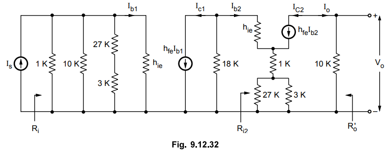

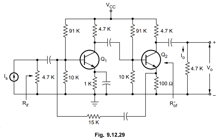
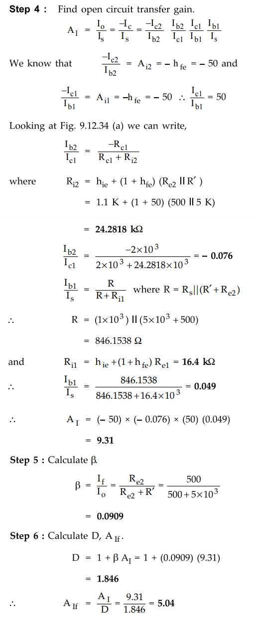
Ex.
9.12.10 For the transistor circuit shown in Fig. 9.12.34 :
i)
Identify the topology of feedback
ii)
Draw equivalent circuit diagram
iii)
Calculate the values of AI β
and AIf. Given for Q1 and Q2 hfe =
50, hie = 1.1 kΩ.

Sol.
: Step 1 : Identify topology
The
feedback is given from emitter of Q2 to the base of Q2. If I = 0 then feedback
current through R'(5 K) register is zero, hence it is current sampling. As
feedback signal is mixed in shunt with input, the amplifier is current shunt
feedback amplifier.
Step
2 and Step 3 : Find input and output circuit. The
input circuit of the amplifier without feedback is obtained by opening the output
loop at the emitter of Q2 (IQ = 0). This places R' (5 K) in series with Rg from
base to emitter of Qr The output circuit is found by shorting the input node,
i.e. making Vi = 0. This places R' (5 K) in parallel with Rg. The resultant
equivalent circuit is shown in Fig. 9.12.34 (a).

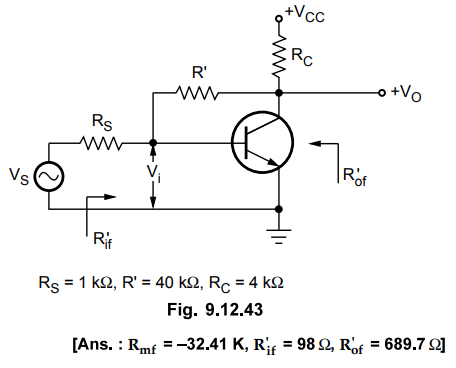
4. Voltage Shunt Feedback
•
Fig. 9.12.35 shows a common emitter amplifier with a resistor R' connected from
the output to the input.

Step
1 :
Identify topology
By
shorting output voltage (V =0), feedback reduces to zero and hence it is a
voltage sampling. As P = Js - Jf, the mixing is shunt type and topology is
voltage shunt feedback amplifier.
Step
2 and Step 3 : Find input and output circuit. To find
input circuit, set V = 0, this places R' between base and ground. To find
output circuit, set V = 0, this places R' between collector and ground. Since
it is a shunt feedback we use Norton's equivalent of the source, i.e. current
source.
The
resultant circuit is shown in Fig. 9.12.36.
•
The feedback signal is the current If in the resistor R' which is in the output
circuit as shown in the Fig. 9.12.36.

Step
4 :
Replace transistor with its h-parameter equivalent circuit.

Substituting
values of equation (9.12.16) and (9.12.17) in equation (9.12.15) we have
Simple
way to calculate R'of
Ex.
9.12.11 For the transistor feedback amplifier shown,

Sol.
:
Step
1 :
Identify topology
By
shorting output voltage (V =0), feedback reduces to zero and hence it is a
voltage sampling. As -i = Is - If, the mixing is shunt type and topology is
voltage shunt feedback amplifier.
Step
2 and Step 3 : Find input and output circuit. To find
input circuit, set V = 0, this places R' between base and ground. To find
output circuit, set V = 0, this places R' between collector and ground. Since
it is a shunt feedback we use Norton's equivalent of the source, i.e. current source.
•
The resultant circuit with transistor replaced by h-parameter equivalent is as
shown in the Fig. 9.12.39.

Step 4 : Find the open circuit transresistance

Ex.
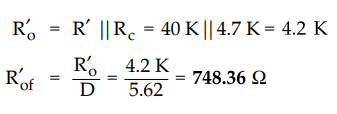
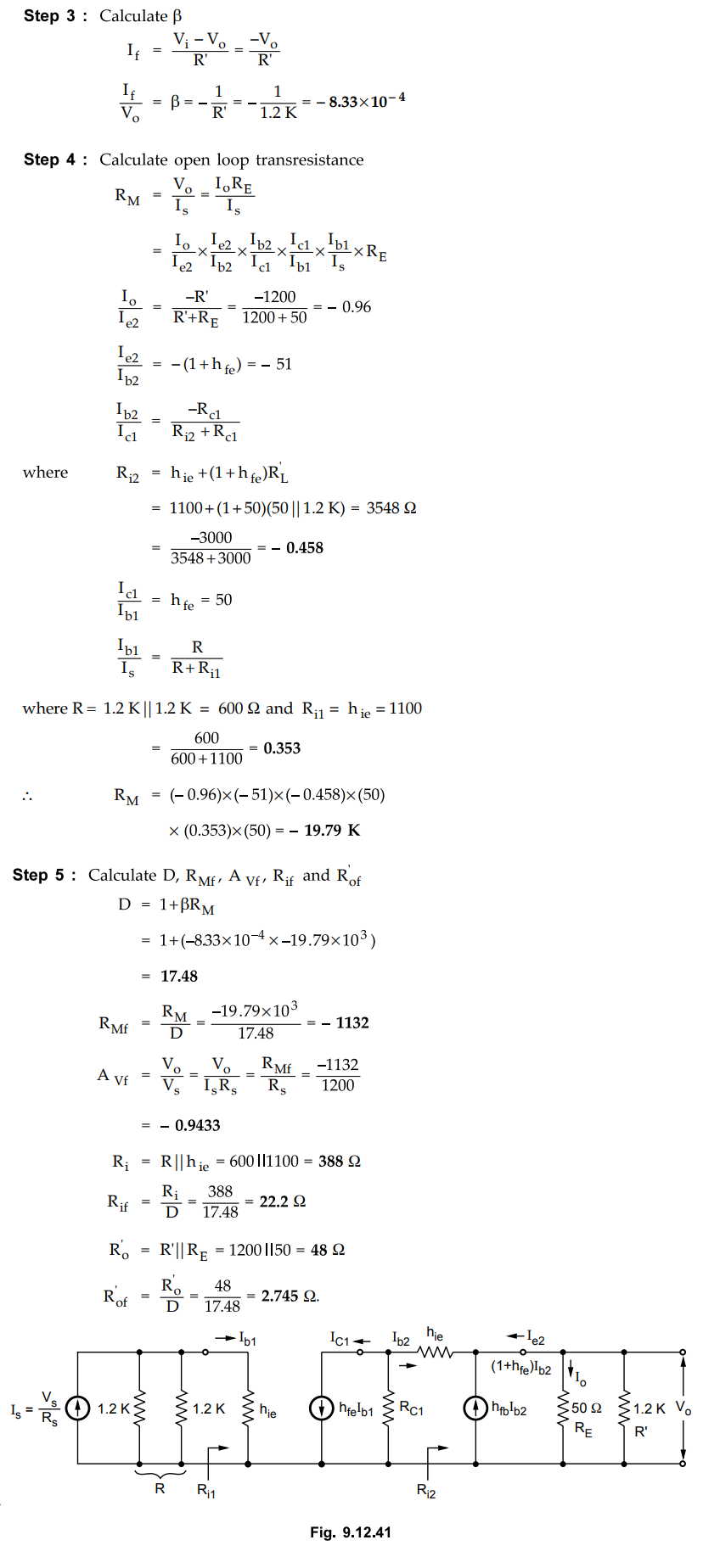
9.12.12 For the transistor amplifier stage shown in Fig. 9.12.40, hfe = 50, hie
= 1.1 K, hre = hoe = 0. Analyse the circuit for : i) Type
of feedback ii) β iii) RM iv) RMF V) AVf vi) RiF vii) RoF.

Sol.
: Step 1 : Identify topology
By
shorting output voltage (Vo = 0), feedback reduces to zero and hence it is a
voltage sampling. As Ii = Is -If, the mixing is shunt type and hence topology
is voltage shunt feedback amplifier.
Step
2 :
Find the h-parameter equivalent circuit
Step
3 :
Calculate β
Examples
for Practice
Ex.
9.12.13 For the transistor feedback amplifier shown,
h
Ex.
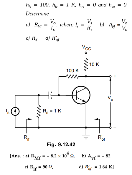
9.12.14 For the transistor feedback stage shown in
Fig.
9.12.43 assume hfe = 100, he = 1.1 K,hoe = hoe
= 0.
1)
Identify the topology with justification.
2)
Calculate Rmf, Rif, Rof.
Review Questions
1. Draw example circuit for each type of feedback.
AU : ECE : May-06, Marks 6
2. Explain the current series feedback amplifier with a neat
diagram.
3. Draw the circuit for voltage series feedback pair and derive
expressions for Rif Rof and Aif.
4. Draw the circuit for common emitter configuration with
unbypassed Rg and derive the expressions for Rif Rof and
Aif.
AU : ECE : Hay-13, Marks 16
5. Draw the circuit for current shunt feedback and derive the
expression for Rif Rof , Avf and Aif
6. Draw the basic circuit of the voltage shunt feedback
amplifier and describe the concepts involved in such an amplifier.
AU : ECE : Dec.-05, Marks 8
7. Determine Ry^^A,, and A^ for the following : i) Voltage shunt
feedback amplifier ii) Current series feedback amplifier.
AU : Dec.-14, Marks 16
8. Draw circuit of CE amplifier with current series feedback and
obtain the expression for feedback ratio, voltage gain, input and output
resistances.
AU : May-15, Marks 16
9. Sketch the circuit diagram of a two-stage capacitor coupled
BJT amplifier that uses series voltage negative feedback. Briefly explain how
the feed back operates.
AU : Dec.-15, Marks 16
Electron Devices and Circuits: Unit V: (a) Feedback Amplifiers : Tag: : - Analysis of Feedback Amplifiers
Related Topics
Related Subjects

Electron Devices and Circuits
EC3301 3rd Semester EEE Dept | 2021 Regulation | 3rd Semester EEE Dept 2021 Regulation