Electron Devices and Circuits: Unit III: (a) BJT Amplifiers
Analysis of Transistor Amplifier Configurations using Simplified h-parameter Model
Solved Example Problems | BJT Amplifiers
• In most practical cases it is appropriate to obtain approximate values of current gain, voltage gain, input and output impedances rather than to carry out more lengthy exact calculations.
Analysis of Transistor Amplifier Configurations using Simplified
h-parameter Model
AU
: Dec.-16
•
In most practical cases it is appropriate to obtain approximate values of
current gain, voltage gain, input and output impedances rather than to carry
out more lengthy exact calculations.
•
As mentioned earlier, if hoe RL < 0.1 then we can
proceed for approximate analysis.
•
In above equation, RL is the effective load resistance.
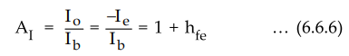
1. Analysis of CE Amplifier using Simplified Hybrid Model
•
Let us consider the h-parameter equivalent circuit for the amplifier, as shown
in the Fig. 6.6.1.

•
In approximate analysis, hoe and hre are neglected.
•
Fig. 6.6.2 shows the approximate h-parameter equivalent circuit. Here, hreVc is
replaced by short circuit and h oe is replaced by open circuit.

Ex.
6.6.1 Consider a single stage CE amplifier with Rs = 1 K, R1=
50 K, R2 = 2 K, RC = 2 K, RL = 2 K, hfe
= 50, hfe = 1.1 K, hoe = 25 µA/V and hre = 2.5
× 10-4, as shown in Fig. 6.6.3.
Find
Ap Ri AV AI = IL / Is = AVs
= Vo / Vs and Ro
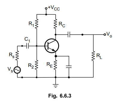
Sol.
:
Since hoe R'L = 25
x 10-6 × (2 K || 2 K) = 0.025, which is less than 0.1, we use
approximate analysis.
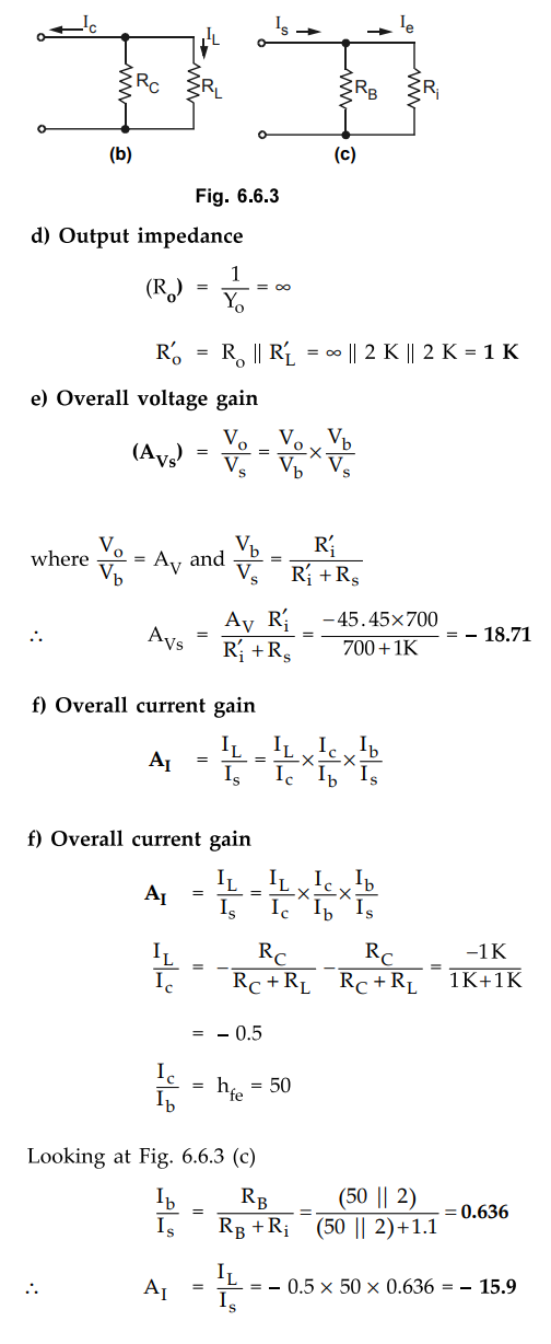
Fig.
6.6.3 (a) shows the simplified hybrid model for the given circuit.
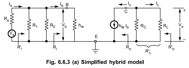
Current
gain :
(AI
) = - hfe = - 50
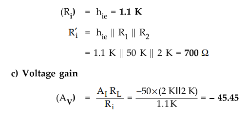
Input
impedance :
Ex.
6.6.2 For CE amplifier with voltage divider bias and bypassed RE, hfe
= 50, hie = 1100 Ω,hre = 2.5 × 10⁻⁴, hoe = 24
µA/V, R1 = 8.2 Ω. R2 = 1.6 kΩ, RC = 1.5 kΩ, RE
= 220Ω, Rs = 1 kΩ, RL = 4.7 kΩ. Assume that all capacitor
trends to infinite. Find Av, AVs, AI, AIs, Rt, Ro, Ri , Ro.
Sol.
:
Since hoe RL = hoe(RC||RL)
=
24 × 10-6(1.5 K||4.7K) = 0.0273, which is less than 0.1, we use
approximate analysis.
a)
Current gain (AI) = -hfe
= - 50
b)
Input resistance (Ri) =
hie = 1100Ω

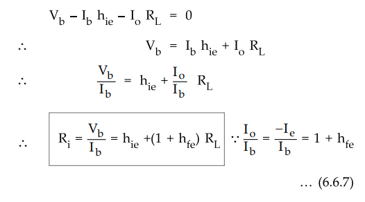
2. Analysis of CC Amplifier using Simplified Hybrid Model
•
We have seen the simplified CE model, in which input is applied to base and
output is taken from collector, and emitter is common between input and output.
•
The same simplified model can be modified to get simplified CC model. For
simplified CC model, we have to make collector common and take the output from
emitter, as shown in the Fig. 6.6.4.
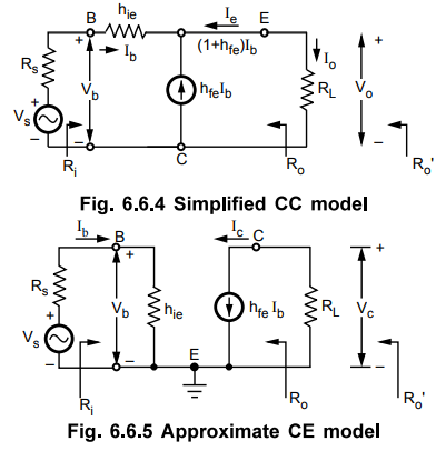
•
The hfe Ib current direction is now exactly opposite that
of CE model because the current hfe Ib always points
towards emitter.
Current
Gain :
Input
Resistance :
Applying
KVL to the outer loop of Fig. 6.6.4 we have,
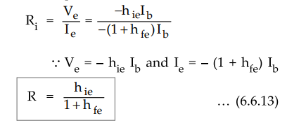
Important
Concept
The
above equation shows that input impedance of CC is higher than the CE
configuration.
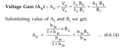
Voltage
Gain (Av) :
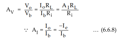
Substituting
values of AI and R1 we get,

Applying
KVL to the outer loop of Fig. 6.6.4 we have,
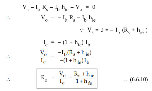
The
output resistance Ro of the stage, taking the load into account is
given as
R’o
= Ro || RL ...
(6.6.11)
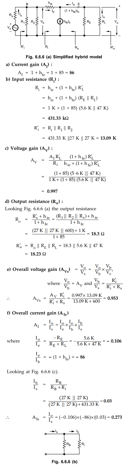
Ex.
6.6.3 A common collector circuit as shown in Fig. 6.6.6 has the following
components : R1 = 27kΩ, R2 = 27kΩ, RE = 5.6 kΩ,
RL = 47kΩ, R5 = 600Ω , The transistor parameters are hie
= 1 kΩ, hfe = 85 and Hoe = 2 µA/V. Calculate AT, Rp Ro,
AVs = Vo / Vs and A = Io /
Io
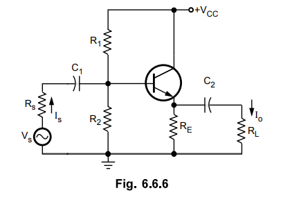
Sol.
:
•
Here, hoe × R'L =
2 × 10-6 × (5.6 || 47K) = 0.01, which is less than 0.1. Thus we
analyse the circuit with approximate method.
•
Fig. 6.6.6 (a) shows the simplified hybrid model for the given circuit.
3. Analysis of CB Amplifier using Simplified Hybrid Model
•
The approximate CB model can be drawn by giving input to emitter, taking output
from collector and making base common. The Fig. 6.6.7 shows the approximate CB
model.
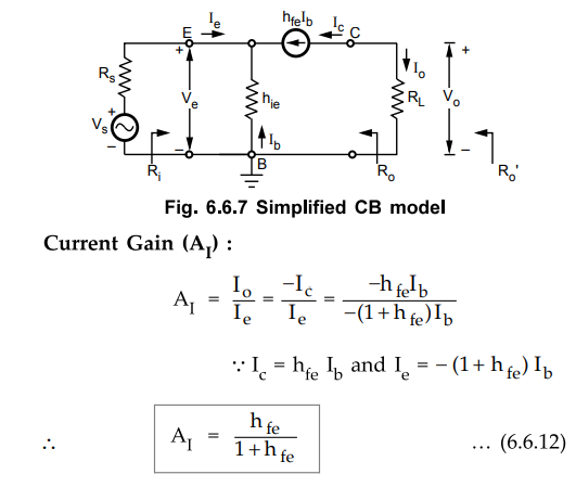
Important
Concept
The
above equation of CB shows that its current gain is always less than one.
Input
Resistance (Ri) :
Important
Concept
The
above equation of CB shows that its input resistance is very low as compare to
CE and CC configurations.
Voltage
Gain (Av) :
Output
Resistance (Ro) : Ro = Vo / Ic | Vs
= 0
When
Vs = 0, the current through input loop Ib =
0, hence Ic = 0 and Ro = ∞
The
output resistance Ro of the stage, taking the load into
account is given as
Ro
= Ro || RL = ∞ || RL =
RL …. (6.6.15)
Ex.
6.6.4 A common base amplifier, as shown in Fig. 6.6.8 has the following
components : Rs = 600 Ω, RC = 5.6 K, RE = 5.6
K, RL = 39 K. The transistor parameters are hie = 1 K, hie
= 85 and hoe = 2 µA/V. Calculate Ri , Ro
, AV, AVS = Vo / VS
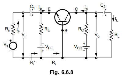
Sol.
:
•
Since hoe × (RC || RL) = 2 × 10-6
× (5.6 K || 39 k Ω) = 9.79 × l0-3, which is
less than 0.1, we use approximate analysis method. The Fig. 6.6.8 (a) shows the
simplified hybrid model for the given circuit.

Electron Devices and Circuits: Unit III: (a) BJT Amplifiers : Tag: : Solved Example Problems | BJT Amplifiers - Analysis of Transistor Amplifier Configurations using Simplified h-parameter Model
Related Topics
Related Subjects

Electron Devices and Circuits
EC3301 3rd Semester EEE Dept | 2021 Regulation | 3rd Semester EEE Dept 2021 Regulation