Linear Integrated Circuits: Unit III: Applications of Op-amp
Antilog Amplifier using Op-amp
Working Principle, Circuit Diagram | Operational amplifier
The log amplifier can easily be turned around to provide the antilog or exponential function which is called antilog amplifier. The basic antilog amplifier can be obtained by using a transistor.
Antilog Amplifier
Dec.-14,
16
The log amplifier can easily be turned around to provide the antilog or exponential function which is called antilog amplifier. The basic antilog amplifier can be obtained by using a transistor.
1. Basic Antilog Amplifier using Transistor
The
same circuit providing antilog of the input can be obtained by using a
transistor instead of a diode. This is shown in the Fig. 3.3.1.

The
node B is at virtual ground hence VB = 0. Thus both collector and
base of the transistor are at ground potential and VCB = 0. Hence
the voltage across the transistor is VBE and we can write the expression for
its collector current as,
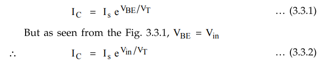
Now
the current IC and current I are same as op-amp input current is zero.

Thus
the output voltage is proportional to the exponential of Vin i.e.
antilog of Vin Thus circuit works as basic antilog amplifier.
In
both the above circuits, it can be seen that the terms Io, Is and VT are
present in the output equation. All these are the function of temperature.
Hence as temperature changes, these parameters also change and cause serious
errors at the output. So the basic antilog circuits also face the same
limitations as that of basic log amplifier circuits. And hence temperature
compensation is must for the antilog amplifier circuits as well.
2. Temperature Compensated Antilog Amplifier
The
circuit of transistor based antilog amplifier with temperature compensation is
shown in the Fig. 3.3.2.
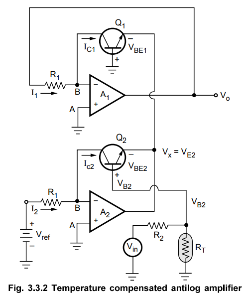
The
two matched transistors Q1 and Q2 are used. The external
voltage Vref is connected to inverting terminal of op-amp A2
through resistance R1. The voltage divider receives the input
voltage Vin. The thermistor RT is used in the voltage
divider.
As
shown in the Fig. 3.3.2,
VB2
= Voltage of base of Q2
VE2
= Voltage of emitter of Q2 = Vx
Let
us derive the expression for the output voltage Vo
For
both the op-amps, as node A is grounded, node B is at virtual ground and hence
VB for both the op-amps is zero.
Referring
to the equation (3.2.3) of section 3.2.1, we can write the equations for
base-emitter voltages of Q1 and Q2 as,

Thus
the output is proportional to the antilog (ln-1) of the
input. And the term RT/VT (R2 + RT
) is constant though temperature changes as RT also changes proportional to the
changes in VT . Thus a complete temperature compensation is achieved
with this circuit.
Review Questions
1. Derive th
expression for antilog amplifier with necessary diagram.
Dec.-14, Marks 5
2. Explain the circuit
operation of temperature compensated antilog amplifier.
3. Write a note on
antilog amplifier using op-amp.
Dec.-16, Marks 7
Linear Integrated Circuits: Unit III: Applications of Op-amp : Tag: : Working Principle, Circuit Diagram | Operational amplifier - Antilog Amplifier using Op-amp
Related Topics
Related Subjects

Linear Integrated Circuits
EE3402 Lic Operational Amplifiers 4th Semester EEE Dept | 2021 Regulation | 4th Semester EEE Dept 2021 Regulation