Microprocessors and Microcontrollers: Unit III: (a) 8051 Microcontroller
Architecture of 8051
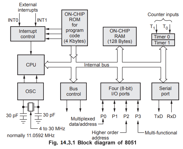
Fig. 14.3.1 shows the internal block diagram of 8051. It consists of a CPU, two kinds of memory sections (data memory - RAM and program memory - EPROM/ROM), input/output ports, special function registers and control logic needed for a timer / counter serial port and interrupt functions.
Architecture of 8051
AU
: May-06,08,09,10,11,12,13,16,17,18, Dec.-04,09,10,11,14,19
Fig.
14.3.1 shows the internal block diagram of 8051. It consists of a CPU, two
kinds of memory sections (data memory - RAM and program memory - EPROM/ROM),
input/output ports, special function registers and control logic needed for a
timer / counter serial port and interrupt functions. These elements communicate
through an eight bit data bus which rims throughout the chip referred as
internal data bus. This bus is buffered to the outside world through an I/O
port when memory or I/O expansion is desired.
1. Central Processing Unit (CPU)
The
CPU of 8051 consists of eight-bit arithmetic and logic unit with associated
registers like A, B, PSW, SP, the sixteen bit program counter and "Data
pointer" (DPTR) registers. Along with these registers it has a set of
special function registers.
The
unique feature of the 8051 architecture is that the ALU can also manipulate one
bit as well as eight-bit data types.
2. A and B CPU Registers
Register
A (Accumulator)
It
is an 8-bit register called accumulator. It holds a source operand and receives
the result of the arithmetic instructions (addition, subtraction,
multiplication and division).
Several
functions apply exclusively to the accumulator : Rotate, parity computation,
testing for zero and so on.
Register
B
In
addition to accumulator, an 8-bit B-register is available as a general purpose
register. It is used for the hardware multiply/divide operation.

3. Data Pointer (DPTR)
The
data pointer (DPTR) consists of a high byte (DPH) and a low byte (DPL). Its
function is to hold a 16-bit address. It may be manipulated as a 16-bit data
register or as two independent 8-bit registers. It serves as a base register in
indirect jumps, lookup table instructions and external data transfer. The DPTR
does not have a single internal address; DPH (83H) and DPL (82H) have separate
internal addresses.
4. The program counter
The
8051 has a 16-bit program counter. It is used to hold the address of memory
location from which the next instruction is to be fetched.
5. 8051 Flag Bits and the PSW Register
The
Fig. 14.3.2 shows the bit pattern of Program Status Word (PSW) of 8051. PSW is
also known as flag register.
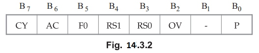
The
8051 consists of following flags.
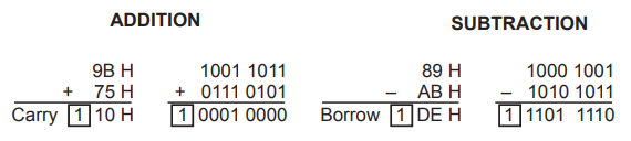
•
CY-Carry Flag : This flag is set if there is an
overflow out of bit 7. The carry flag also serves as a borrow flag for
subtraction. In both the examples shown below, the carry flag is set.
•
AC-Auxiliary Carry Flag : This flag is set if there is an
overflow out of bit 3 i.e., carry from lower nibble to higher nibble (D3
bit to D4 bit).
•
FO
- Available for user for general purpose.
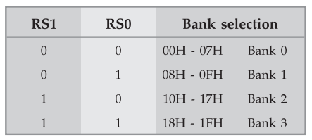
•
RS1 - RS0 (Register Bank Select) : They select the
working register bank as follows:
•
OV-Over Flow Flag : This flag is set whenever the result of
a signed number operation is too large, causing the high-order bit to overflow
into the sign bit.
•
P-Parity Flag : Parity is defined by the number of ones
present in the accumulator. P = 0, if number of ones are even and P = 1, if
number of ones are odd.
Example
:
The status of CY, AC and P flags after the addition of 9BH and 65H is as
follows :
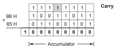
CY
= 1, AC = 1 and P = 0
There
are instructions in 8051, that tests the condition of flags in the PSW register
and make decision based on the status of flags. Thus, programmer use these
flags to perform some arithmetic operations which involves carry or borrow, or
to change the program control (using conditional branching).
As
mention earlier, programmer can select register bank by setting corresponding
bits in PSW.
6. Special Function Register of 8051
The
group of registers, implemented to perform special functions and are located
immediately above the 128 bytes of RAM are called special function registers.
All access to the four I/O ports, the CPU registers, interrupt control
registers, the timer/counter, UART and power control are performed through
registers between 80H and FFH.
Special
Function Registers (SFRs) are a sort of control table used for running and
monitoring the operation of the microcontroller. Each of these registers as
well as each bit they include, has its name, address in the scope of RAM and
precisely defined purpose such as timer control, interrupt control, serial
communication control etc.
Even
though there are 128 memory locations intended to be occupied by them, the
basic core, shared by all types of 8051 microcontrollers, has only 21 such
registers. Rest of locations are intentionally left unoccupied in order to
enable the manufacturers to further develop microcontrollers keeping them
compatible with the previous versions.
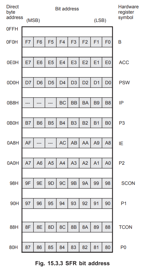
Fig.
14.3.3 shows special function bit addresses
Table
14.3.1 contains a list of all the SFRs and their addresses and their value in
binary at reset.
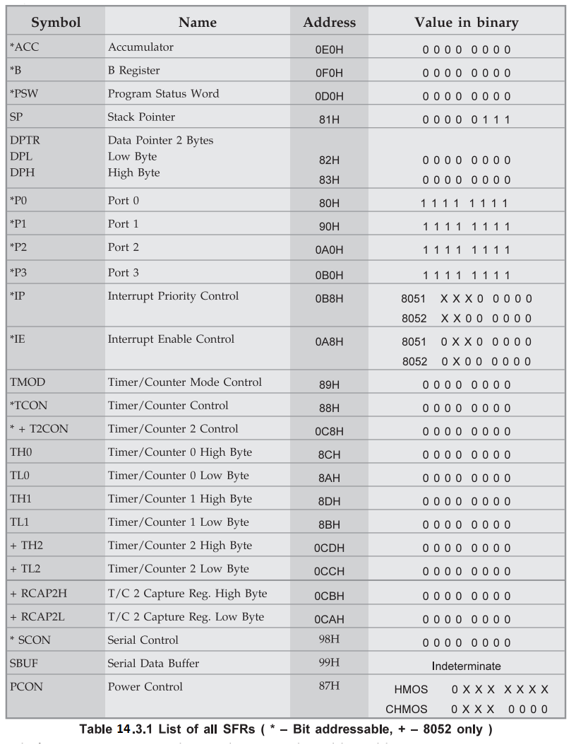
*
before register name indicates that it is a bit addressable.
+
before register name indicates that it is supported by only 8052.
Review Questions
1. Give the details of
PSW of 8051.
AU : May-10, Dec.-19,
Marks 2
2. Quantify the number
of register banks in 8051 and say how the CPU knows which bank is currently in
use. AU: Dec.-10
3. Explain the
functional block diagram of 8051 in detail AU: Dec.-04,09,
May-09,10 Marks 10
4. Describe the
architecture of 8051 with neat diagram. AU: May-06,08,11,12,17, Marks 16
5. List the on-chip
peripherals of 8051 microcontroller.
6. Mention the size of
DPTR and stack pointer in 8051 microcontroller. AU : Dec.-11, Marks 2
7. What is program
status word of 8051 ? AU: May-11, Marks 2 AU: May-12, Marks 2
8. Explain with a neat
block diagram the architecture of8051 microcontroller. AU : May-13, 16, 18,
Marks 16
9. Explain the functional block diagram of 8051 microcontroller.
Microprocessors and Microcontrollers: Unit III: (a) 8051 Microcontroller : Tag: : - Architecture of 8051