Microprocessors and Microcontrollers: Unit I: (a) 8085 Processor
Architecture of 8085
Questions : 1. With neat functional block diagram, explain the architecture of 8085 microprocessor.2. Define the function of parity flag and zero flag in 8085.3. Explain the architecture, data flow and instruction execution of 8085 microprocessor. 4. Briefly describe stack pointer register. 5. With neat block diagram explain the various functional building blocks of 8085 processor
Architecture of 8085
AU
: May-04, 10, 11, 12, 16, 17, 18, Dec.-04, 07, 08, 09, 10, 13, 15, 16, 17, 18,
19, June-06, 12
Fig. 1.2.1 shows the architecture of 8085.

It
consists of various functional blocks as listed below :
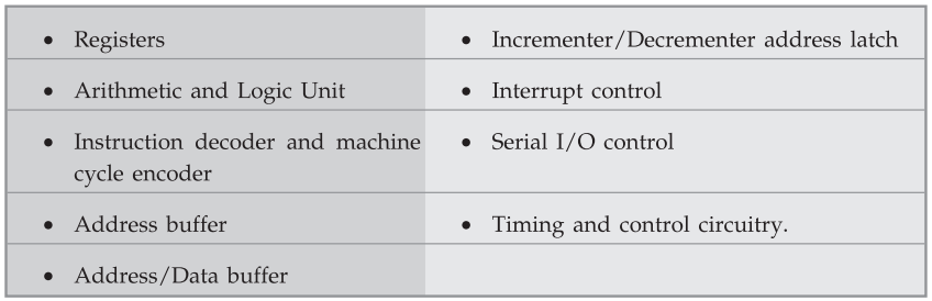
•
Registers • Incrementer/Decrementer
address latch
•
Arithmetic and Logic Unit • Interrupt control
•
Instruction decoder and machine cycle encoder •
Serial I/O control
•
Address buffer • Timing and control
circuitry.
•
Address/Data buffer
1. Register Structure
 The
Fig. 1.2.2 shows the register structure of 8085. The shaded portion of this
register model is called programmer's model of 8085. It includes six 8-bit
registers- (B, C, D, E, H and L) one accumulator, one flag register and two
16-bit registers (SP and PC). All these registers are accessible to programmer
and hence they are included in the programmer's model. The remaining registers
- temporary, W and Z are not accessible to the programmers; they are used by
microprocessor for internal, intermediate operations.
The
Fig. 1.2.2 shows the register structure of 8085. The shaded portion of this
register model is called programmer's model of 8085. It includes six 8-bit
registers- (B, C, D, E, H and L) one accumulator, one flag register and two
16-bit registers (SP and PC). All these registers are accessible to programmer
and hence they are included in the programmer's model. The remaining registers
- temporary, W and Z are not accessible to the programmers; they are used by
microprocessor for internal, intermediate operations.
1.
General Purpose Registers :
C,
D, E, H and L are 8-bit general purpose registers can be used as a separate
8-bit registers or as 16-bit register pairs, BC, DE and HL. HL pair also
functions as a data pointer or memory pointer.
2.
Special Purpose Registers :
a)
Register A (Accumulator) : It is a tri-state eight bit
register. It is extensively used in arithmetic, logic, load and store
operations, as well as in, input/output (I/O) operations. Most of the times the
result of arithmetic and logical operations is stored in the register A. Hence
it is also identified as accumulator.
b)
Flag Register : It is an 8-bit register, in which five
of the bits carry significant information in the form of flags : S (Sign flag),
Z (Zero flag), AC (Auxiliary Carry flag), P (Parity flag), and CY (Carry flag),
as shown in Fig. 1.2.3.
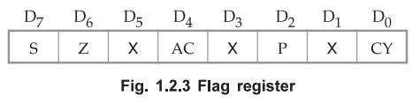
S-Sign
flag : After the execution of arithmetic or logical
operations, if bit D7 of the result is 1, the sign flag is set. In a
given byte if D7 is 1, the number will be viewed as negative number.
If D7 is 0, the number will be considered as positive number.
Z-Zero
flag : The zero flag sets if the result of operation in
ALU is zero and flag resets if result is non zero. The zero flag is also set if
a certain register content becomes zero following an increment or decrement
operation of that register.
AC-Auxiliary
Carry flag : This flag is set if there is an
overflow out of bit 3 i.e. , carry from lower nibble to higher nibble (D3
bit to D4 bit). This flag is used for BCD operations and it is not
available for the programmer.
P-Parity
flag : Parity is defined by the number of ones present in
the accumulator. After an arithmetic or logical operation if the result has an
even number of ones, i.e. even parity, the flag is set. If the parity is odd,
flag is reset.
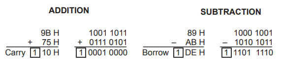
CY-Carry
flag : This flag is set if there is an overflow out of bit
7. The carry flag also serves as a borrow flag for subtraction. In both the
examples shown below, the carry flag is set.
c)
Instruction Register : In a typical processor operation,
the processor first fetches the opcode of instruction from memory (i.e. it
places an address on the address bus and memory responds by placing the data
stored at the specified address on the data bus). The CPU stores this opcode in
a register called the instruction register. This opcode is further sent to the
instruction decoder to select one of the 256 alternatives.
d)
Program Counter (PC) : Program is a sequence of
instructions. As mentioned earlier, microprocessor fetches these instructions
from the memory and executes them sequentially. The program counter is a
special purpose register which, at a given time, stores the address of the next
instruction to be fetched. Program Counter acts as a pointer to the next
instruction. How processor increments program counter depends on the nature of
the instruction; for one byte instruction it increments program counter by one,
for two byte instruction it increments program counter by two and for three
byte instruction it increments program counter by three such that program
counter always points to the address of the next instruction.
e)
Stack Pointer (SP) : The stack is a reserved area of the
memory in the RAM where temporary information may be stored. A 16-bit stack
pointer is used to hold the address of the most recent stack entry.
2. Arithmetic Logic Unit (ALU)
The
8085's ALU performs arithmetic and logical functions on eight bit variables.
The arithmetic unit performs bitwise fundamental arithmetic operations such as
addition and subtraction. The logic unit performs logical operations such as
complement, AND, OR and EX-OR, as well as rotate and clear. The ALU also looks
after the branching decisions.
3. Instruction Decoder and Machine Cycle Encoder
The
instruction decoder decodes the opcode and accordingly gives information to the
timing and control circuit.
The
8085 executes seven different types of machine cycles. It gives the information
about which machine cycle is currently executing in the encoded form on the S0,
S1 and ppppppppp lines. This task is done by machine cycle encoder.
4. Address Buffer
This
is an 8-bit unidirectional tristate buffer. It is used to drive external high
order address bus (A15-A8).
5. Address/Data Buffer
This
is an 8-bit bi-directional buffer. It is used to drive multiplexed address/data
bus, i.e. low order address bus (A7 – A0) and data bus (D7
– D0).
6. Incrementer/Decrementer Address Latch
This
16-bit register is used to increment or decrement the contents of program
counter or stack pointer.
7. interrupt control
The interrupt control block has five interrupt
inputs RST 5.5, RST 6.5, RST 7.5, TRAP and INTR and one acknowledge signal  .
It controls the interrupt activity of 8085 microprocessor.
.
It controls the interrupt activity of 8085 microprocessor.
8. serial I/O control
The
8085's serial I/O control provides two lines, SOD and SID for serial
communication. The serial output data (SOD) line is used to send data serially
and serial input data (SID) line is used to receive data serially.
9. Timing and Control Circuitry
The
control circuitry in the processor 8085 is responsible for all the operations.
The control circuitry and hence the operations in 8085 are synchronized with
the help of clock signal. Along with the control of fetching and decoding
operations and generating appropriate signals for instruction execution,
control circuitry also generates signals required to interface external devices
to the processor, 8085.
10. Instruction Execution and Data Flow in 8085
•
In order to execute program, the starting address of the program is loaded into
the Program Counter (PC).
•
The 8085 sends the contents of PC as an address on the address bus and
activates ![]() control signal.
control signal.
•
Upon receiving the address and ![]() signal memory puts the contents of
addressed memory location on the data bus which is an opcode of an instruction.
Meanwhile, PC is incremented to point the next memory location in the program
sequence.
signal memory puts the contents of
addressed memory location on the data bus which is an opcode of an instruction.
Meanwhile, PC is incremented to point the next memory location in the program
sequence.
• ![]() signal is deactivated and opcode is loaded into the instruction
register via internal bus of microprocessor.
signal is deactivated and opcode is loaded into the instruction
register via internal bus of microprocessor.
•
The instruction decoding unit decodes the instruction and provides information
to the timing and control unit to generate necessary signals for instruction
execution.
Review Questions
1. With neat
functional block diagram, explain the architecture of 8085 microprocessor.
AU : June-06,
Dec.-04,07, 08,09,10,19, May-04,10,11,12, Marks 16
2. Draw and explain
the architecture of 8085.
3. Give the format of
flag register in 8085. Explain each flag.
4. Define the function
of parity flag and zero flag in 8085.
5. Explain the
architecture, data flow and instruction execution of 8085 microprocessor.
AU : May-11, Marks 8
6. Explain with a neat
block diagram the architecture of 8085 microprocessor.
AU : May-12, 16,
Dec.-15, 16, 17, Marks 12
7. Explain the
registers of 8085 microprocessor.
8. Briefly describe
stack pointer register.
9. With neat block
diagram explain the various functional building blocks of 8085 processor
AU : May-18, Dec.-18, Marks 13
Microprocessors and Microcontrollers: Unit I: (a) 8085 Processor : Tag: : - Architecture of 8085
Related Topics
Related Subjects
Microprocessor and Microcontroller
EE3404 MCU 4th Semester EEE Dept | 2021 Regulation | 4th Semester EEE Dept 2021 Regulation