Linear Integrated Circuits: AU Solved Paper
AU Solved Paper - set 1
Linear Integrated Circuits
Linear Integrated Circuits: AU Solved Paper : Semester - III (EEE)
AU Solved Paper
December-2014
Linear Integrated Circuits and Applications
Semester - III (EEE)
Time
:
Three Hours]
[Maximum
Marks : 100
Answer
ALL questions.
PART
A - (10 × 2 = 20 Marks)
Q.1
What are the major categories of integrated circuits ?
(Refer
Two Marks Q.3 of Chapter-1)
Q.2
Mention the advantages of integrated circuits over discrete circuits.
(Refer
Two Marks Q.l of Chapter-1)
Q.3
Draw an adder circuit using an op-amp to get the output expression as
Vo
= (0.1 V1 + V2 + 10 V3) where V1,V2
and V3 are the inputs.
(Refer
Two Marks Q.75 of Chapter-2)
Q.4
A 100 pF capacitor has a maximum charging current of 150 microamps. What is the
slew rate ?
(Refer
Two Marks Q.76 of Chapter-2)
Q.5
Draw the fundamental sample and hold circuit. What is the purpose of S/H in
data converters ?
(Refer
Two Marks Q.72, Q.73 of Chapter-3)
Q.6
How many comparators are required to design a 10 bit flash ADC ?
(Refer
Two Marks Q.107 of Chapter-3)
Q.7
A PLL frequency multiplier has an input frequency of and a decade counter is included
in the loop. What will be the frequency of the PLL output ?
(Refer
Two Marks Q.50 of Chapter-3)
Q.8
What are the advantages of variable transconductance technique ?
(Refer
Two Marks Q.57 of Chapter-4)
Q.9
What is meant by thermal shutdown applied to voltage regulators ?
(Refer
Two Marks Q.40 of Chapter-5)
Q.10
Draw the internal block diagram of a function generator IC.
(Refer
Two Marks Q.41 of Chapter-5)
PART
B - (5 × 16 = 80 Marks)
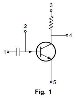
Q.11
i) Explain the fabrication process involved in the following circuit diagram
(Fig. 1).
(Refer
section 1.15) [10]
ii)
Explain the process of masking and photo etching in IC fabrication.
(Refer
section 1.8) [6]
OR
b)
i) Discuss the different ways to fabricate diodes.
(Refer
section 1.14)
ii)
Explain how a monolithic capacitor can be fabricated.
(Refer
section 1.14)
Q.12
a) i) Consider the lossy integrator as shown in Fig. 2. For the component
values R1 = 10 kΩ, R = 100 kΩ, C = 1 µF, Determine the lower frequency limit of
integration and study the response for the inputs
1)
Step input 2) Square input 3) Sine input.
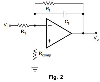
(Refer
example 2.29.3) [10]
ii) Design an adder-subtractor circuit for Vo = 2V1 + 5V2 - 10V3
(Refer
example 2.28.3) [6]
OR
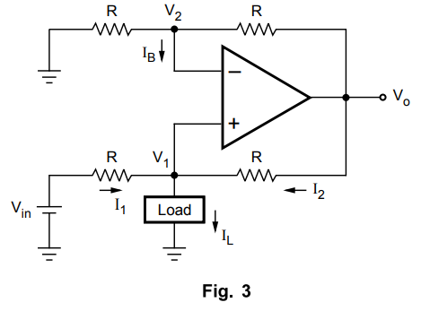
b)
i) For a V-I convertor shown in Fig. 3, Vin - 5 V, R - 10 kΩ, V1
– 1V, find the load current and output voltage Vo. Assume the op-amp
is initially nulled.
(Refer
example 2.25.1) [6]
ii)
For a maximum frequency of 100 Hz, design a differentiator circuit and draw the
frequency response for the same.
(Refer
example 2.30.1) [10]
Q.13 a) i) A dual slope ADC uses 16-bit counter and 4 MHz clock rate. The maximum input voltage is + 10 V. The maximum integrator output voltage should be - 8 V when the counter has cycled through 2n counts. The capacitor used in the integrator is 0.1 pF . Find the value of resistor R of the integrator.
(Refer
example 3.26.7) [6]
ii)
Derive the expression for the log and antilog amplifiers with necessary diagrams.
(Refer
sections 3.2.1 and 3.3.1) [10]
OR
b)
i) In a triangular wave generator given R2 = 1.2 kΩ, R3 = 6.8 kΩ, R2
= 120 kΩ, C2 = 0.01 pF. Determine the peak to peak output amplitude
of triangular wave and frequency of the triangular wave.
(Refer
example 3.20.2) [8]
ii)
Design a RC phase shift oscillator for a frequency of 1 kHz.
(Refer
example 3.17.1) [8]
Q.14
a) i) For the VCO circuit, assume R2 = 2.2 kΩ,R1 = R3
= 15 kΩ and C1 = 0.001 µF. Assume VCC = 12 V. Determine
the output frequency, the change in output frequency if modulating input VC
is varied from 7 V to 8 V.
(Refer
example 4.2.1) [8]
ii)
For a 555 astable circuit, determine the high state time interval, low state
time interval, period, frequency and duty cycle.
(Refer
section 4.1.3) [8]
OR
b)
With neat diagram, explain the operation of four quadrant variable
transconductance multiplier circuit.
(Refer
section 4.7) [16]
Q.15
a) i) State the advantages of IC voltage regulator. Explain the features and
internal structure of general purpose linear 1C 725 regulator. Design a
regulator using IC 723 to meet the following specifications : Vo = 5
V; Io = 100 mA;
Vin
= 15 ±20 %; Isc = 150 mA; Vsense = 0.7 V
(Refer
sections 5.6, 5.7.1, 5.7.2 and example 5.7.1) [8]
ii)
With a neat diagram, explain the working of step down switching regulator.
(Refer
section 5.12.3) [8]
OR
b)
i) With a neat functional diagram, explain the operation of LM 380 power
amplifier.
(Refer
section 5.14.3) [8]
ii)
Explain the operation of SMPS with neat diagrams.
(Refer
section 5.12.1) [8]
Linear Integrated Circuits: AU Solved Paper : Tag: : Linear Integrated Circuits - AU Solved Paper - set 1
Related Topics
Related Subjects

Linear Integrated Circuits
EE3402 Lic Operational Amplifiers 4th Semester EEE Dept | 2021 Regulation | 4th Semester EEE Dept 2021 Regulation