Linear Integrated Circuits: AU Solved Paper
AU Solved Paper - set 6
Linear Integrated Circuits
Linear Integrated Circuits: AU Solved Paper : Semester - III (EEE)
AU Solved Paper [71766]
May - 2017
Linear Integrated Circuits and Applications
Semester - III (EEE)
Regulation 2013
Time
: Three Hours] [Maximum Marks : 100
Answer
ALL questions.
PART
A - (10 × 2 = 20 Marks)
Q.1
State the advantages of CMOS circuits.
(Refer
Two Marks Q.63 of Chapter - 1)
Q.2
What is lithography ?
(Refer
Two Marks Q.29 of Chapter - 1)
Q.3
Draw the circuit diagram of a symmetrical emitter coupled differential
amplifier.
(Refer
Two Marks Q.80 of Chapter - 2)
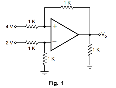
Q.4
For the circuit diagram shown below determine the output voltage V0.
(Refer
Two Marks Q.81 of Chapter - 2)
Q.5
Draw the circuit diagram of a zero cross detector with input and output
waveforms.
(Refer
Two Marks Q.124 of Chapter - 3)
Q.6
Which is the fastest ADC ? State reason.
(Refer
Two Marks Q.110 of Chapter-3)
Q.7
What is an analog multiplier ? Name its applications.
(Refer
Two Marks Q.26 of Chapter - 4)
Q.8
Define the circuit diagram of a PLL circuit used as an AM modulator.
(Refer
section 4.5.5)
Q.9
Give one comparison for switching regulator and variable voltage regulator.
(Refer
Two Marks Q.45 of Chapter - 5)
Q.10
How are frequency of triangular waveform, obtained using ICL 8038 function
generator ?
(Refer
Two Marks Q.46 of Chapter - 5)
PART B - (5 × 13 = 65 Marks)
Q.11
a) With neat illustrations explain the various steps involved in the IC
fabrication process.
(Refer
section 1.15) [13]
OR
b)
With circuit diagram explain the steps involved in the fabrication of the
circuit shown below using IC technology.
(Refer
section 1.15) [13]
OR
b)
With circuit diagram explain the steps involved in the fabrication of the
circuit shown below using IC technology.
(Refer
section 1.15) [13]
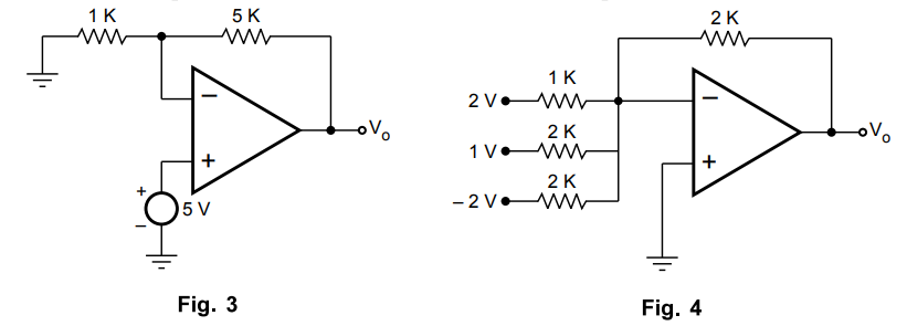
Q.12
a) Determine the output voltage for the following circuits. [13]
i)
(Refer example 2.22.1) ii) (Refer example 2.27.1)
OR
b)
i) With diagram explain the working principle of V/I converter.
(Refer
section 2.25) [5]
ii)
Write a note on stability criterion and compensation techniques applicable to
apamp circuit.
(Refer
sections 2.31 and 2.33) [8]
Q.13
a) With diagram explain the following applications of op amp. [13]
i)
Clippers and clampers (Refer sections 3.21 and 3.22)
ii)
Triangular waveform generator. (Refer section 3.20)
OR
b)
i) Explain the working principle of R-2R ladder type D/A converter.
(Refer
section 3.25.2.3) [7]
ii)
Design a second order Butterworth low pass filter with cut off frequency 2 kHz.
(Refer
example 3.7.2) [6]
Q.14
a) Briefly explain the functional block diagram of NE 565 PLL-IC to operate as
a frequency divider.
(Refer
sections 4.5.1 and 4.5.2) [13]
OR
b)
i) Explain the functional block diagram of 555 timer IC.
(Refer
section 4.1.1) [8]
ii)
Design a monostable multivibrator with pulse duration of 1 msec using 555 timer
IC.
(Refer example 4.1.2) [5]
Q.15
a) With necessary diagram and waveforms explain the working principle of
switched mode power supply.
(Refer
section 5.12) [13]
OR
b)
Write short notes on the following :
i)
LM 380 power amplifier (Refer section 5.14)
ii)
ICE 8038 function generator. (Refer section 5.15) [13]
PART
C - (1 × 15 = 15 Marks)
Q.16
a) Sketch the implementation of an instrumentation amplifier using three
opamps. Explain the principle of operation and its applications.
(Refer
sections 3.1.2 and 3.1.3) [15]
OR
b)
Using 7805 design a current source to deliver a 0.2 A current to a 22 Ohm 10 W
load.
(Refer
example 5.9.4) [15]
Linear Integrated Circuits: AU Solved Paper : Tag: : Linear Integrated Circuits - AU Solved Paper - set 6
Related Topics
Related Subjects

Linear Integrated Circuits
EE3402 Lic Operational Amplifiers 4th Semester EEE Dept | 2021 Regulation | 4th Semester EEE Dept 2021 Regulation