Linear Integrated Circuits: Unit III: Applications of Op-amp
Band Elimination Filter using Op-amp
Classification, Working Principle, Circuit Diagram | Operational amplifier
As mentioned earlier, this filter is also called band stop filter or band reject filter. The action of this filter is exactly opposite to the band pass filter. This filter has two pass bands and one stop band. A band of frequencies is attenuated by this filter, hence the name band elimination filter.
Band Elimination Filter
As
mentioned earlier, this filter is also called band stop filter or band reject
filter. The action of this filter is exactly opposite to the band pass filter.
This filter has two pass bands and one stop band. A band of frequencies is
attenuated by this filter, hence the name band elimination filter.
This
filter is also classified as :
i)
Wide band reject filter and
ii)
Narrow band reject filter.
The
figure of merit (Q) for narrow band filter is greater than 10. In its frequency
response, it shows a notch and hence, also called as notch filter. The
bandwidth of the notch filter is very small as compared to wide band reject
filter.
1. Wide Band Reject Filter
Similar
to the wide band pass filter, this filter also consists of a high pass and low
pass filter sections. Additionally, it consists of a summing amplifier. The
Fig. 3.11.1 shows the circuit diagram of wide band reject filter.
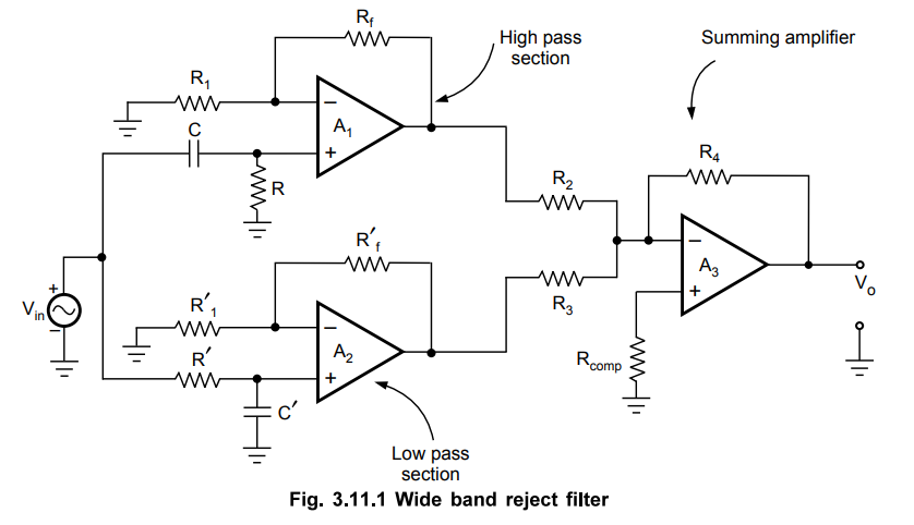
To
have the satisfactory operation of this filter, it has to satisfy following two
conditions :
i)
The low cut-off frequency, fL of high pass filter must be greater
than the high cut-off frequency, fH of low pass filter.
ii)
The pass band gain of both high pass and low pass sections must be equal. The
design of the overall filter is based on the individual design of the various
sections.
The
gain of the summing amplifier can be set to 1 for simplicity and thus,
R2
= R3 = R4 = R ….
(3.11.1)
Hence,
Rcomp = R2 || R3 || R4 = R / 3 …. (3.11.2)
Both
high pass and low pass sections provide attenuation in the stop band between fH
and fL. For f < fH the transmission is due to low pass
section while for f > fL, the transmission is due to high pass
section. The frequency response for this type of filter is shown in Fig.
3.11.2.

The
centre frequency, fC is given by,
fC
= √fH fL
2. Narrow Band Reject Filter (Notch Filter)
The
name of the filter i.e. Notch filter is due to the characteristics shape of its
frequency response curve. The stop band of this filter is very narrow. The
typical application of the notch filter is the rejection of a single frequency,
such as 50 Hz power line frequency hum. It is also used in the biomedical
instrumentation and also blanking of control tones for telephone lines. Thus,
particular unwanted frequency can be eliminated using this filter.
The
passive circuit used to obtain the notch filter is the twin T network as shown
in Fig. 3.11.3.

It
consists of two T networks. One consists of two resistors and a capacitor while
other consists of two capacitors and one resistor.
The
notch out frequency is the frequency at which the maximum attenuation occurs.
This is given by
fN
= 1 / 2πRC … (3.11.3)
The
value of Q i.e. figure of merit for the passive network is very low, hence an
active notch filter which uses twin T network is preferred in practice. This is
shown in Fig. 3.11.4.
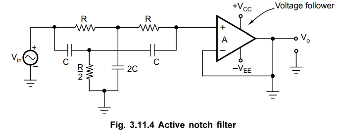
To
design a notch filter, to eliminate the specific notch frequency, fN
choose the capacitor C less than or equal to µF. Then, calculate the value of R
using equation (3.11.3). To obtain best performance of the circuit, the
components designed should have precise values which are close to their
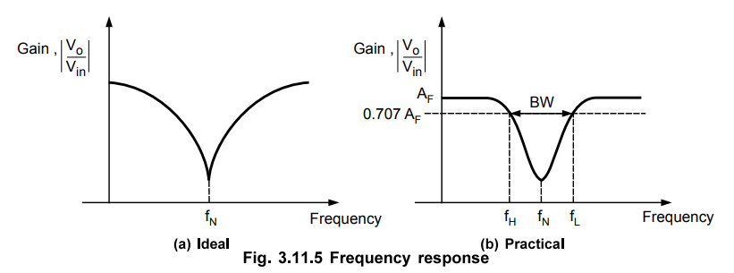
designed values. The frequency response of the notch filter is shown in the
Fig. 3.11.5. Fig. 3.11.5 (a) shows the ideal response while the Fig. 3.11.5 (b)
shows the practical response.
Review Questions
1. What is band
elimination filter ? Draw its frequency response.
2. What is a notch
filter ? Explain its operation with the help of a neat circuit diagram.
Linear Integrated Circuits: Unit III: Applications of Op-amp : Tag: : Classification, Working Principle, Circuit Diagram | Operational amplifier - Band Elimination Filter using Op-amp
Related Topics
Related Subjects

Linear Integrated Circuits
EE3402 Lic Operational Amplifiers 4th Semester EEE Dept | 2021 Regulation | 4th Semester EEE Dept 2021 Regulation