Microprocessors and Microcontrollers: Unit I: (d) Memory Interfacing
Basic Concepts in Memory Interfacing with 8085
Memory Interfacing
For interfacing memory devices to microprocessor 8085, following important points are to be kept in mind.
Basic Concepts in Memory Interfacing with 8085
AU
: Dec.-05, 07, 10, 11, 16, May-08, 10, 11, 17
For
interfacing memory devices to microprocessor 8085, following important points
are to be kept in mind.
1.
Microprocessor 8085 can access 64 kbytes memory since address bus is 16-bit.
But it is not always necessary to use full 64 kbytes address space. The total
memory size depends upon the application.
2.
Generally EPROM (or EPROMs) is used as a program memory and RAM (or RAMs) as a
data memory. When both, EPROM and RAM are used, the total address space 64
kbytes is shared by them.
3.
The capacity of program memory and data memory depends on the application.
TECHNICAL
PUBLICATIONS - An up thrust for knowledge
4.
It is not always necessary to select 1 EPROM and 1 RAM. We can have multiple
EPROMs and multiple RAMs as per the requirement of application. For example: We
have to implement 32 kbytes of program memory and 4 kbytes EPROMs are
available. In this case, we can connect 8 EPROMs in parallel (4 kbytes × 8 = 32
kbytes) with different chip select for each EPROM.
5.
We can place EPROM/RAM anywhere in full 64 kbytes address space. But program
memory (EPROM) should be located from address 0000H since reset address of 8085
microprocessor is 0000H.
6.
It is not always necessary to locate EPROM and RAM in consecutive memory
addresses. For example : If the mapping of EPROM is from 0000H to OFFFH,
it is not must to locate RAM from 1000H. We can locate it anywhere between
1000H and FFFFH. Where to locate memory component totally depends on the
application.
Memory
Interfacing Requirements
•
Select the chip.
•
Identify the register.
•
Enable the appropriate buffer.
Microprocessor
system includes memory devices and I/O devices. It is important to note that
microprocessor can communicate (read/write) with only one device at a time,
since the data, address and control buses are common for all the devices. In
order to communicate with memory or I/O devices, it is necessary to decode the
address from the microprocessor. Due to this each device (memory or I/O) can be
accessed independently. The following section describes common address decoding
techniques.
Address
Decoding Techniques
•
Absolute decoding/Full decoding.
•
Linear decoding/Partial decoding.
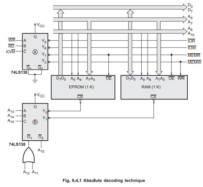
Absolute
decoding
In
absolute decoding technique, all the higher address lines are decoded to select
the memory chip, and the memory chip is selected only for the specified logic
levels on these high-order address lines; no other logic levels can select the
chip. Fig. 6.4.1 shows the memory interface with absolute decoding. This
addressing technique is normally used in large memory systems.
Memory Map :

Linear
decoding
In
small systems, hardware for the decoding logic can be eliminated by using
individual high-order address lines to select memory chips. This is referred to
as linear decoding. Fig. 6.4.2 shows the addressing of RAM with linear decoding
technique. This technique is also called partial decoding. It reduces the cost
of decoding circuit, but it has a drawback of multiple addresses (shadow
addresses).
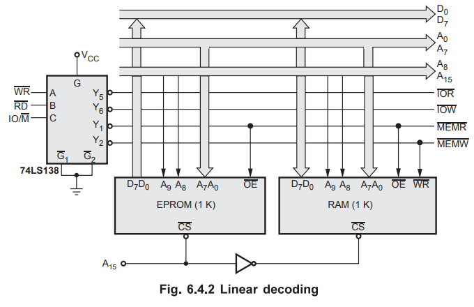
Fig.
6.4.2 shows the addressing of RAM with linear decoding technique. A15
address line, is directly connected to the chip select signal of EPROM and
after inversion it is connected to the chip select signal of the RAM.
Therefore, when the status of A15 line is 'zero', EPROM gets
selected and when the status of A15 line is 'one' RAM gets selected.
The status of the other address lines is not considered, since those address
lines are not used for generation of chip select signals.
Memory
Map :


1. Interfacing Examples
Example
6.4.1 Design memory system for the 8085 microprocessor
such that it should contain 8 kbyte of EPROM (Erasable Programmable Read Only
Memory) and 8 kbyte of RAM ( Read/Write Memory).
Solution
:
Fig. 6.4.3 shows the desired memory system using IC 2764 (8 K) EPROM and 6264
(8 K) RAM. Memory requires 13 address lines (A0-A12)
since 213 = 8 K. The remaining address lines (A13 - A15
) are decoded to generate chip select  signals. IC 74LS138 is used
as decoder. When ( A15 - A13 ) address lines are zero,
the Yo output of decoder goes low and selects the EPROM. This means that A15
- A13 address lines must be zero to read data from EPROM. The
address lines A12 – A0 select the particular memory
location in the EPROM when A15 - A13 lines are zero. Similarly,
when address lines A15 - A13 are 001, the Y1 output of
decoder goes low and selects the RAM. The Table 6.4.3 shows the memory map for
the designed circuit.
signals. IC 74LS138 is used
as decoder. When ( A15 - A13 ) address lines are zero,
the Yo output of decoder goes low and selects the EPROM. This means that A15
- A13 address lines must be zero to read data from EPROM. The
address lines A12 – A0 select the particular memory
location in the EPROM when A15 - A13 lines are zero. Similarly,
when address lines A15 - A13 are 001, the Y1 output of
decoder goes low and selects the RAM. The Table 6.4.3 shows the memory map for
the designed circuit.
Memory
Map :


Example
6.4.2 Design a microprocessor system for the 8085
microprocessor such that it should contain 16 kbyte of EPROM and 4 kbyte of RAM
using two 8 kbyte EPROMs (2764) and two 2 kbyte RAMs (6116).
Solution
:
Fig. 6.4.4 (See on next page) shows the desired memory system using two (8 K ×
8) EPROM and two (2 K × 8) RAMs. EPROM memory is 8 K, so it requires 13 address
lines (A12 - A0) whereas RAM memory is 2 K, so it
requires 11 address lines (A10 - Ao). The remaining higher address lines (A15
- A13) are used to generate chip-select signals. Table
6.4.4 shows the memory map for the designed circuit.

Memory
Map :

Example
6.4.3 Design a microprocessor system for the 8085
microprocessor such that it should contain 2 kbyte of EPROM and 2 kbyte of RAM
with starting addresses 0000H and 6000H respectively.
Solution
:
Fig. 6.4.5 (See on next page) shows the desired memory system using 2 kbyte
EPROM and 2 kbyte RAM. Both EPROM and RAM are 2 K, so they require 11 address
lines (A10 – A0). The remaining hi gher address lines (A15
- A11) are used to generate chip select signals.
The
chip selection logic is designed to have starting address of EPROM, 0000H and
starting address of RAM, 6000H. This is implemented by selecting EPROM only
when higher address lines (A15 - A11) are all zero, and
selecting RAM only when higher address lines (A15 - A11)
are 01100 (Binary). The Table 6.4.5 shows the memory map for the designed
circuit.
Memory
Map :


Example
6.4.4 Interface a 8K × 8 EPROM IC and 2K × 8 RAM IC
with 8085 such that the starting address assigned to them are 0000H and 4000H
respectively using address decoder having NAND gate and inverters.
AU:
Dec.-07, Marks 8
Solution
: Fig.
6.4.6 shows the desired memory system using 8 K EPROM and 2 K RAM. EPROM
requires 13 address lines (A, A12). Since 213 = 8K and RAM requires
11 address lines. (A0 - A10) since 211 = 2 K.
The remaining address lines (A15 - A13) are inverted and
given as NAND input to generate chip select signal. So that when
(A15 - A13)
address lines are zero, EPROM is selected. The address lines A0 - A12
select the particular memory location in the EPROM when A15 - A13
lines are zero. Similarly, when address lines A11, A12, A13,
A15 are zero and A14 is one, RAM is selected.

Memory
Map :

Example
6.4.5 With necessary diagram explain the interfacing
of a RAM memory IC 6116 (2K × 8) with 8085.
AU
: May-11, Marks 8
Solution
: Fig. 6.4.7 shows the
desired memory system using 2K RAM. The 2K RAM requires 11 address lines (A0
- A10) since 211 = 2 K. Let us assume that the RAM is located
at 4000H to 47FFH in the memory. To address the RAM in the desired range the
remaining address lines A11 - A15 are used. The ![]() signal is generated using inverters and NAND gate such that it will remain low
for entire address range (4000H - 47FFH).
signal is generated using inverters and NAND gate such that it will remain low
for entire address range (4000H - 47FFH).

Review Questions
1. With necessary
diagrams, write short notes RAM memory interfacing and ROM memory interfacing
AU : May-08, Marks 16
2. Design a
microprocessor system to interface an 8K × 8 EPROM and 8K × 8 RAM.
AU : Dec.-05, Marks 8
3. Explain the
interfacing of memory with 8085 microprocessor.
4. Interface a 8KX8
EPROM IC and 2KX8 RAM IC with 8085 such that the starting address assigned to
them are 0000H and 4000H respectively using address decoder having NAND gate
and inverters.
AU : Dec.-07, Marks 8
5. How address
decoding is done in memory interface.
6. With necessary
diagram, explain the interfacing of a RAM memory IC-6H6 (2K × 8) with 8085.
AU : May-11, Marks 8
7. List the steps
involved in interfacing a memory to the 8085 microprocessor.
AU : Dec.-10, Marks 2
8. Draw the
interfacing diagram to interface 8085 with 2 KB RAM and 4 KB EPROM.
AU : Dec.-16, Marks 8
9. What is meant by memory interfacing ? Explain with an example.
Microprocessors and Microcontrollers: Unit I: (d) Memory Interfacing : Tag: : Memory Interfacing - Basic Concepts in Memory Interfacing with 8085