Linear Integrated Circuits: Unit IV: Special ICs
Basic PLL Operation
Operating working principle, Features, Block Diagram, Circuit Diagram, Functions
Fig. 4.3.1 shows the block diagram of PLL. It consists of • Phase detector • Low pass filter • Error amplifier • Voltage Controlled Oscillator (VCO)
Basic PLL Operation
Fig.
4.3.1 shows the block diagram of PLL. It consists of
•
Phase detector
•
Low pass filter
•
Error amplifier
•
Voltage Controlled Oscillator (VCO)

The
phase detector compares the input frequency fs with the feedback
frequency fo and generates an output signal which is a function of
the difference between the phases of the two input signals. The output signal
of the phase detector is a dc voltage. The output of phase detector is applied
to low pass filter to remove high frequency noise from the dc voltage. The
output of low pass filter without high frequency noise is often referred to as
error voltage or control voltage for VCO. When control voltage is zero, VCO is
in free-running mode and its output frequency is called as center frequency fo.
The non-zero control voltage results in a shift in the VCO frequency from its
free-running frequency, fo to a frequency fo given by f = fo
+ Kv VC where Kv is the voltage to frequency
transfer coefficient of the VCO. The error or control voltage applied as an
input to the VCO, forces the VCO to change its output frequency in the
direction that reduces the difference between the input frequency and the output
frequency of VCO.
This
action, commonly known as capturing, continues till the output frequency of VCO
is same as the input signal frequency. Once the two frequencies are same, the
circuit is said to be locked. In locked condition, phase detector generates a
constant dc level which is required to shift the output frequency of VCO from
centre frequency to the input frequency. Once locked, PLL tracks the frequency
changes of the input signal. Thus, a PLL goes through three states : Free
running, capture and phase lock.
1. Important Definitions Related to PLL
Some
important definitions related to PLL are as follows :
Lock
Range : When PLL is in lock, it can track frequency changes
in the incoming signal. The range of frequencies over which the PLL can maintain
lock with the incoming signal is called the lock range or tracking range of the
PLL. It is usually expressed as a percentage of fo, the VCO
frequency.
Capture
Range : The range of frequencies over which the PLL can
acquire lock with an input signal is called the capture range. It is also
expressed as a percentage of fo.
Pull-In
Time : The capture of an input signal does not take place
as soon as the signal is applied, but it takes finite time. The total time
taken by the PLL to establish a lock is called pull-in time. This depends on
the initial phase and frequency difference between the two signals as well as
on the overall loop again and the bandwidth of the low pass filter.
2. Close Loop Analysis of PLL
Under
locked conditions a linear relationship can exist Vs between the output voltage
of os the phase detector and the phase difference between the VCO and the input
signal if the later is small. The nonlinearity of phase detector makes the PLL
nonlinear.
Here,
we assume linear PLL in the lock condition and analyse it using standard linear
feedback concept. The Fig. 4.3.2 shows the block diagram of PLL system,

Where Kϕ : Conversion gain of phase detector in
volt/rad
F(s)
: Loop filter transfer function
A
: Gain of the amplifier
Kv
: Voltage to frequency transfer coefficient of VCO
The phase of the VCO output is actually equal to the time integral of the VCO output frequency,
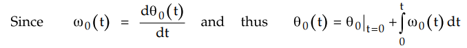
Thus,
an integration inherently takes place within the PLL. This integration is
represented by the 1/s block in the Fig. 4.3.2.
In
practice, when the VCO input voltage, Vf is zero, the VCO frequency
is not zero. The VCO frequency when Vf = 0 is called VCO free
running frequency we or center frequency ωc. The relation between
the VCO output frequency ω0 and Vf is given by
ω0
(t) = ωc +K0Vf(t)
The
close loop transfer function for a PLL system shown in the Fig. 4.3.2 is given
by

where
KL = KϕKVA and it is known as loop bandwidth.
In terms of the loop parameters, KL, is simply the product of the phase
detector gain, Kϕ, VCO transfer coefficient, and the electrical gain
provided by the amplifier.
Review Questions
1. Draw the block
diagram of basic PLL and explain the function of each block.
May-07, Marks 8, Dec.-07, Marks 10
2. Perform the closed
loop analysis of PLL.
May-12, Marks 8
3. Define capture
range.
Dec.-03, 04, 08, 10, Marks 2
4. Define lock-range.
Dec.-04, 08, 10, May-05, Marks 2
5. Define pull-in
time.
Dec.-04, Marks 2
6. What is PLL?
Dec.-16, Marks 2
Linear Integrated Circuits: Unit IV: Special ICs : Tag: : Operating working principle, Features, Block Diagram, Circuit Diagram, Functions - Basic PLL Operation
Related Topics
Related Subjects

Linear Integrated Circuits
EE3402 Lic Operational Amplifiers 4th Semester EEE Dept | 2021 Regulation | 4th Semester EEE Dept 2021 Regulation