Electron Devices and Circuits: Unit II: (a) Bipolar Junction Transistors (BJT)
Biasing of BJT
Bipolar Junction Transistors
• The transistor can be operated in three regions : cut-off, active and saturation by applying proper biasing conditions as shown in the Table 2.5.1.
Biasing of BJT
AU
: Dec.-14, 15
•
The transistor can be operated in three regions : cut-off, active and
saturation by applying proper biasing conditions as shown in the Table 2.5.1.
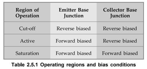
Table
2.5.1 Operating regions and bias conditions
•
In order to operate transistor in the desired region we have to apply external
d.c. voltages of correct polarity and magnitude to the two junctions of the
transistor. This is nothing but the biasing of the transistor. Because d.c.
voltages are used to bias the transistor, biasing is known as d.c. biasing of
the transistor.
1. Need for Biasing
•
In transistor amplifier circuits, output signal power is always greater than
input signal power. Now the question is how this amplification of power is
achieved. The d.c. sources (d.c. biasing) supplies the power to the transistor
circuit to get the output signal power greater than input signal power.
•
Thus, we can say that the biasing is needed
• to operate transistor in the desired region
•
to get the output signal power greater than input signal power.
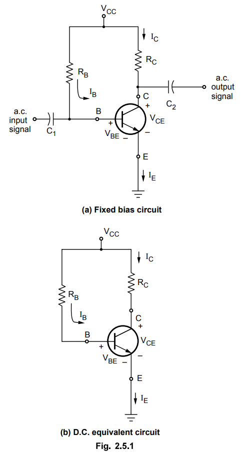
2. Fixed Bias Circuit
•
The Fig. 2.5.1 shows the fixed bias circuit. It is the simplest d.c. bias
configuration. For the d.c. analysis we can replace capacitor with an open
circuit because the reactance of a capacitor for d.c. is
XC
= 1/2π fC =1 /2π (0) C= ∝.
•
The d.c. equivalent of fixed bias circuit is shown in Fig. 2.5.1 (b).
Base Circuit
•
Applying Kirchhoff s voltage law (KVL) to the base circuit shown in Fig. 2.5.2
we get,
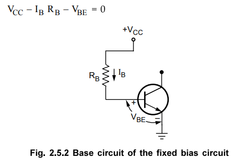
IB = VCC - VBE / RB ... (2.5.1)
Collector
Circuit
•
Applying Kirchhoff's voltage law to the collector circuit shown in Fig. 2.5.3
we get,
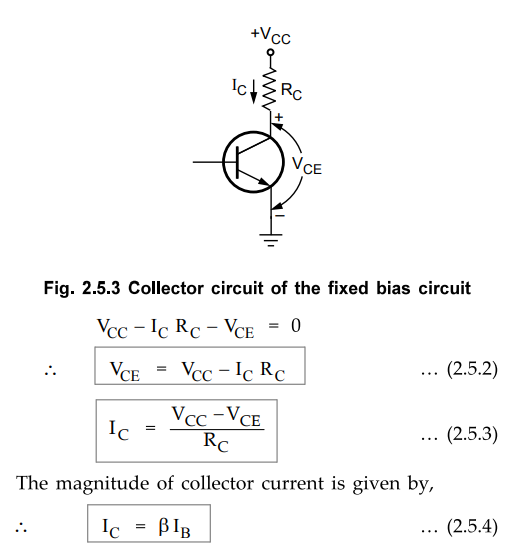
•
It is important to note that since the base current is controlled by the value
of RB and IC is related to IB by a constant P the magnitude of IC is not a function
of the resistance RC.
•
Changing RC to any level will not affect the level o IB or IC as long as we
remain in the active region of the device. However, the change in RC will
change the value of VCE-
VCE
= VC – VE ...
(2.5.5)
•
Where, VC : Collector voltage and VE : Emitter voltage
•
Similarly,
VBE
= VB – VE Where,
VB : Base voltage ... (2.5.6)
•
In this circuit, VE = 0,
VBE
= VB and VCE = VC ... (2.5.7)
Ex.
2.5.1 For the circuit shown in the Fig. 2.5.4. Calculate IB, Ic ,VCE ,VB ,VC
and VBC. Assume VBE = 0.7 V β = 50
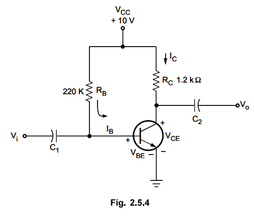
Sol.
:
The
negative voltage VBC indicates that
base-collector
junction is reverse biased.
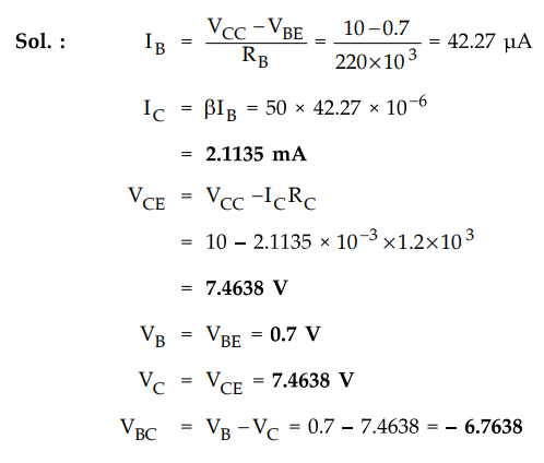
Ex.
2.5.2 Calculate the minimum and maximum values of Ic and VCE for the base bias
when hFE(min) = 50 and hFE(max) = 60 . For circuit, VCC = 12V , RC = 2 K and RB
= 150 K. Assume silicon transistor.
Sol.
:
For silicon transistor VBE = 0-7 V .
Important
Concept
The
transistor manufacturers provide minimum and maximum values of hEE. The example
shows that if the value of hEE varies within the range specified by the
manufacturer bias point will vary in base bias circuit.
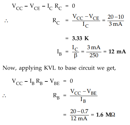
Ex.
2.5.3 Design a fixed bias circuit to have operating point of (10 V, 3 mA); The
circuit is supplied with 20 V and uses a silicon transistor of hfe =
250.
Sol.
:
The Fig. 2.5.5 shows the fixed bias circuit with given values.
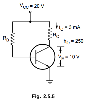
Applying
KVL to collector circuit we get,
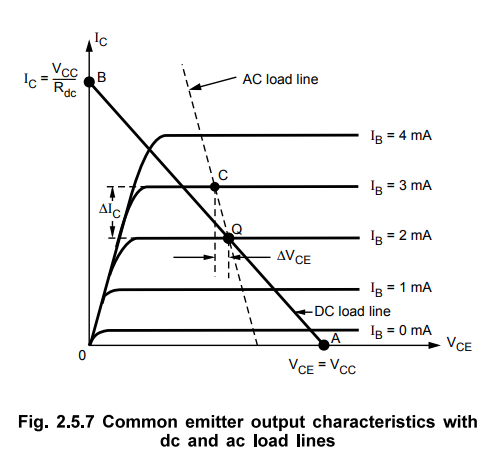
3. DC (Static) Load Line and Quiescent Point
•
For fixed-bias circuit, we have
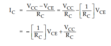
•
By comparing this equation with equation of straight line y = mx + c, where m
is the slope of the line and c is the intercept on Y-axis, then we can draw a
straight line on the graph of Ic versus VCE which is having slope - 1/RC and
Y-intercept Vcc/Rc- To determine the two points on the line we assume VCE
= VCC and VCE = 0.
1.
When VCE = VCC;
Ic
= 0 and we get a point A and
2.
When VCE = 0;
IC
= VCC/RC and we get a point B
•
The Fig. 2.1.6 shows the output characteristics of a common emitter
configuration with points A and B, and line drawn between them. The line drawn
between points A and B is called d.c. load line.
•
The 'd.c.' word indicates that only d.c. conditions are considered, i.e. input
signal is assumed to be zero.
•
The d.c. load line is a plot of Ic versus VCE, for a given value of
RC and a given level of Vcc.
•
Thus, it represents all collector current levels and corresponding
collector-emitter voltages that can exist in the circuit.
•
Knowing any one of IC, IB or VCE, it is easy
to determine the other two from the load line.
•
The slope of the d.c. load line depends on the value of It is negative and
equal to reciprocal of the RC
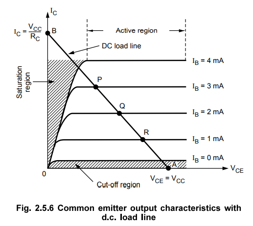
•
For fixed bias circuit, IB = VCC – VBE / RB
•
The intersection of curves of different values of IB with d.c. load line gives
different operating points. For different values of IB, we have different
intersection points (quiescent point or Q point) such as P, Q and R.
•
The operating point can be selected at different positions on the d.c. load
line : near saturation region, near cut-off region or at the center, i.e. in
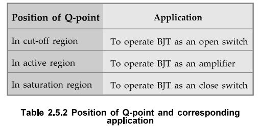
the active region. The selection of operating point will depend on its
application as shown in the Table 2.5.2.
•
The position of the selected operating point is called quiescent point or
Q-point. The co-ordinates of Q-point are : Q = (VCEO,ICO)
4. AC (Dynamic Load Line)
•
Under d.c. conditions C1 and C2 acts as an open circuit.
Hence the quiescent collector current and voltages are obtained by drawing a
static (d.c.) load line corresponding to the resistance RC through the point iC
= 0, vCE = VCC as shown in the Fig. 2.5.6.
•
If RL ≠ ∞ and if the input signal (base current) is large and symmetrical, we
can locate the Q-point at the centre of the load line and the collector voltage
and current may vary approximately symmetrically around the VCEQ and
ICQ, respectively.
•
If RL we have draw a dynamic (a.c.) load line. Because, at the signal frequency
C2 acts as a short circuit and the effective load R'L at the collector is RC m
parallel with RL .
•
When no signal is applied, the transistor voltage and current conditions are as
indicated at the quiescent point (Q point) on the dc load line.
•
When an ac signal is applied, the transistor voltage and current vary above and
below point Q. Therefore, point Q is common to both the ac and the dc load
lines.
•
Starting from the Q point, the ac load line is drawn by taking a convenient
collector current change
Δ
IC = Δ VCE / RL
•
The current and voltage changes are then measured from point Q to obtain
another point on the ac load line. The ac load line is drawn through this point
and point Q as shown in the Fig. 2.5.7.
5. Selection of Operating Point
•
The operating point can be selected at different positions on the d.c. load
line : near saturation region, near cut-off region or at the center, i.e. in
the active region. The selection of operating point will depend on its
application. When transistor is used as an amplifier, the Q point should be
selected at the center of the d.c. load line to prevent any possible distortion
in the amplified output signal. This is well-understood by going through
following cases.
•
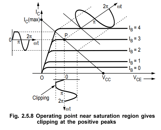
Case 1 : Biasing circuit is designed to fix a Q point at
point P, as shown in Fig. 2.5.8. Point P is very near to the saturation region.
As shown in Fig. 2.5.8 the collector current is clipped at the positive half
cycle. So, even though base current varies sinusoidally, collector current is
not a useful sinusoidal waveform, i.e. distortion is present at the output.
Therefore, point P is not a suitable operating point.
•
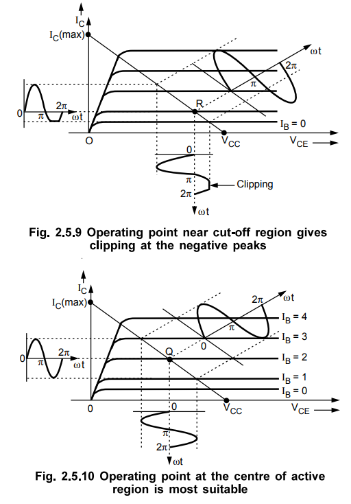
Case 2 : Biasing circuit is designed to fix a Q point at
point R as shown in Fig. 2.5.10. Point R is very near to the cut-off region. As
shown in Fig. 2.5.9 the collector current is clipped at the negative half
cycle. So, point R is also not a suitable operating point.
•
Case 3 : Biasing circuit is designed to fix a Q point at
point Q as shown in Fig. 2.5.10. The output signal is sinusoidal waveform
without any distortion. Thus point Q is the best operating point.
Important
Concept
It
is important to note that effective load R'L (parallel combination of RQ and
RL) is always less than RQ. Therefore, the slope of the ac load line is always
higher than the dc load line.
Review Questions
1. Why biasing is necessary in BJT amplifiers ?
2. What do you understand by Q-point ? What is its significance
?
3. Explain the concept of dc load line with the help of neat
diagram.
4. Draw and explain the ac load line.
5. Explain the selection of Q point for a transistor bias
circuit and discuss the limitations on the output voltage swing.
Electron Devices and Circuits: Unit II: (a) Bipolar Junction Transistors (BJT) : Tag: : Bipolar Junction Transistors - Biasing of BJT
Related Topics
Related Subjects

Electron Devices and Circuits
EC3301 3rd Semester EEE Dept | 2021 Regulation | 3rd Semester EEE Dept 2021 Regulation