Electron Devices and Circuits: Unit II: (b) Junction Field Effect Transistor (JEET)
Biasing of JFET
Solved Example Problems | Junction Field Effect Transistor (JFET)
• Different biasing circuits of JFET are : • Fixed bias circuit • Self bias circuit • Voltage divider bias circuit
Biasing of JFET
•
Different biasing circuits of JFET are :
• Fixed
bias circuit
• Self
bias circuit
• Voltage
divider bias circuit
1. Fixed-bias Circuit
•
Fig. 3.6.1 shows the fixed bias circuit for the n-channel JFET. This is the
simplest biasing arrangement.
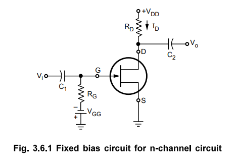
•
To make gate-source junction reverse-biased, a separate supply VGG is connected
such that gate is more negative than the source.
•
For the d.c. analysis coupling capacitors are open circuits. The current
through RG is IG which is zero.
•
This permits RG to replace by short circuit equivalent, simplifying the fixed
bias circuit as shown in the Fig. 3.6.2.

Step
1 : Calculate VGS
•
We know for d.c. analysis IG = 0 A and applying KVL to the input circuit we
get,
VGS
+ VGG = 0
VGS
= - VGG … (3.6.1)
•
Since VGG is a fixed d.c. supply, the voltage VGS is fixed in
magnitude, and hence the name fixed bias circuit.
Step
2 : Calculate IDQ
•
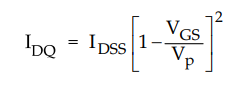
The drain current ID can be calculated using equation.
IDQ
= IDSS (1 – VGS /
VP)2
Step
3 : Calculate VDS
•
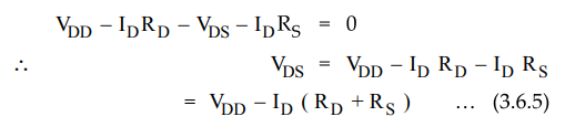
The drain to source voltage of drain circuit can be determined by applying KVL.
VDD
-IDRD - VDSQ = 0
VDSQ = VDD - IDRD
•
The main drawback of fixed bias circuit of FET is that it requires two power
supplies.
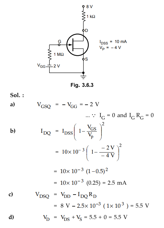
Ex.
3.6.1 For the circuit shown in the Fig. 3.6.3 Calculate :
a)
VGSQ, b) IDQ, c) VDSQ, d) VD
2. Self Bias Circuit
•
Self bias is the most common type of JFET bias. Recall that a JFET must be
operated such that the gate source junction is always reverse-biased.
•
This condition requires a negative VGS for an n-channel JFET and a positive VGS
for p-channel JFET. This can be achieved using the self bias arrangement shown
in Fig. 3.6.4.

• The gate resistor, RG, does not affect the bias because it has essentially no
voltage drop across it; and therefore the gate remains at 0 V.
•
RG is necessary only to isolate an a.c. signal from ground in amplifier
applications.
•
The voltage drop across resistor, Rg makes gate source junction reverse biased.
Step
1 :
Obtain expression for VGS
•
For the n-channel FET in Fig. 3.6.4 (a), Ig produces a voltage drop across Rg
and makes the source positive with respect to ground. Since Ig = ID and VG = 0,
then Vg = Ig Rg = ID Rg. The gate to source voltage is,
VGS
= VG - VS = 0 - ID RS = - IDRS
•
For the p-channel FET in Fig. 3.6.4 (b), Ig produces a voltage drop across Rg
and makes the source negative with respect to ground. Since IS = ID
and VG = 0, then VG = - ISRS = - IDRS.
The gate to source voltage is
VGS
= VG - VS = 0 – (- ID RS ) = + IDRS
•
In the following D.C. analysis, the n-channel JFET shown in Fig. 3.6.4 (a) is
used to for illustration.
•
For D.C. analysis we can replace coupling capacitors by open circuits and we
can also replace the resistor RG by a short circuit equivalent, since IG = 0.
This is illustrated in Fig. 3.6.5.

Ex.
3.6.2 For the circuit shown in Fig. 3.6.6 Calculate VGSQ’ IDQ'
VDS' VS and VD.

Sol.
:
Step
1 : Obtain expression for VGS
VGS
= - IDRS
Step
2 : Calculate ID and Values of VGS and VS.
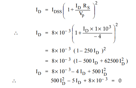
Solving
quadratic equation using formula

•
IDQ cannot have value 8 mA because maximum value of ID IDSS is given
as 8 mA at VGS = 0 and hence IDQ is taken as 2 mA.

Ex.
3.6.3 Calculate the value of feedback resistor (Rs) required to self bias an
N-channel JFET with IDSS = 40 mA, Vp = -10 and VGSQ
= - 5 V.
Sol.
:
Step
1 : Calculate IDQ

Ex.
3.6.4 Vp = - 2 V, 1DSS = 1.65 mA for the circuit in Fig. 3.6.7. It is desired
to bias the circuit at ID = 0.8 mA, VDD = 24 V. Calculate i) VGS ii)
gm iii)RS
Sol.
:

Ex.
3.6.5 The FET shown in Fig. 3.6.8 has |lDSS | =12 mA and \Vp\ = 5 V.
Calculate the quiescent values of i) ID ii) VDS Hi) VGS.
Sol
: Fig 3.6.9 shows simplified circuit for d.c. analysis
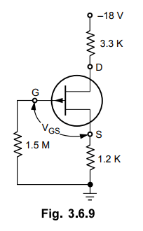
Step
1 : Obtain express for VGS
VGS
- ID RS = 0
VGS
= ID RS
Step
2 : Calculate ID
We
have ID = IDSS (1 – VGS / Vp)2
Substituting
value of VGS in above equation and solving for ID we get,
Practically,
value of VDS for p-channel FET should be negative, hence value of ID
= 7.45 mA is invalid.
.'. ID = 2.33 mA
Step
3 :
Calculate VDS and VGB.
Now
calculating VDS taking ID = 2.33 mA
Ex.
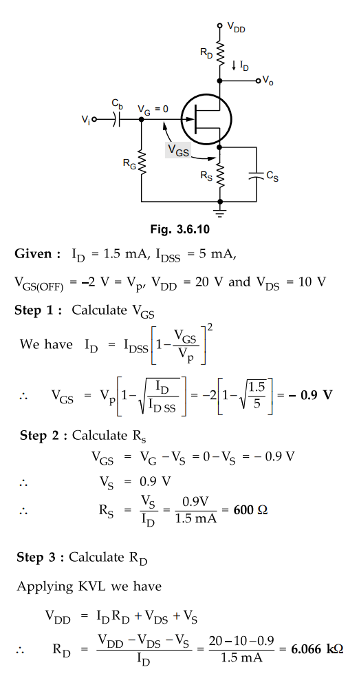
3.6.6 In a self-bias n-channel JFET, the operating point is to be set at ID =
1.5 mA and VDS = 10 V. The parameters are IDSS = 5 mA and Vcs(off) =
V- values of Rs and RD in VDD = 20 V. AU
: Dec.-18, Marks 9
Sol.
:
Fig. 3.6.10 shows the self bias circuit for n-channel JFET.
Examples
for Practice
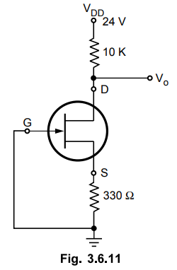
Ex.
3.6.7 : Vp = - 4 V, IDSS = 1.8 mA for the
circuit in Fig. 3.6.11 It is desired to bias the circuit at ID = 0.8 mA, VDD
= 20 V. Calculate VGS

Ex.
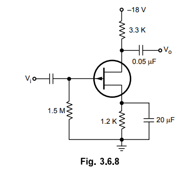
3.6.8 :A FET amplifier shown in Fig. 3.6.12 has the following parameters IDSS =
2 mA, Vp = -2.4 V. Determine i) VGS ii) Q-point.
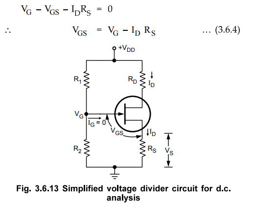
3. Voltage Divider Bias Circuit
•
The Fig. 3.6.12 shows n-channel JFET with voltage divider bias.

•
The voltage at the source of the JFET must be more positive than the voltage at
the gate in order to keep the gate-source junction reverse-biased.
•
The source voltage is,
VS
= I D RS
•
The gate voltage is set by resistors R1 and R2 .
•
Coupling capacitors C1 and C2 and source resistor bypass
capacitor CS are assumed to be open circuit for DC analysis.
Step
1 : Calculate VG
VG
=
VDD R2 / R1 + R2
IG
= 0
Step
2 :
Obtain expression for VGS
• Applying KVL to the input circuit we get,
Step
3 : Calculate IDQ
•
The IDQ can be calculated using equation :
Step
4 : Calculate VDS and VGS
Applying
KVL to the output circuit we get,
•
The Q point of a JFET amplifier using the voltage divider bias is given by :

Ex.
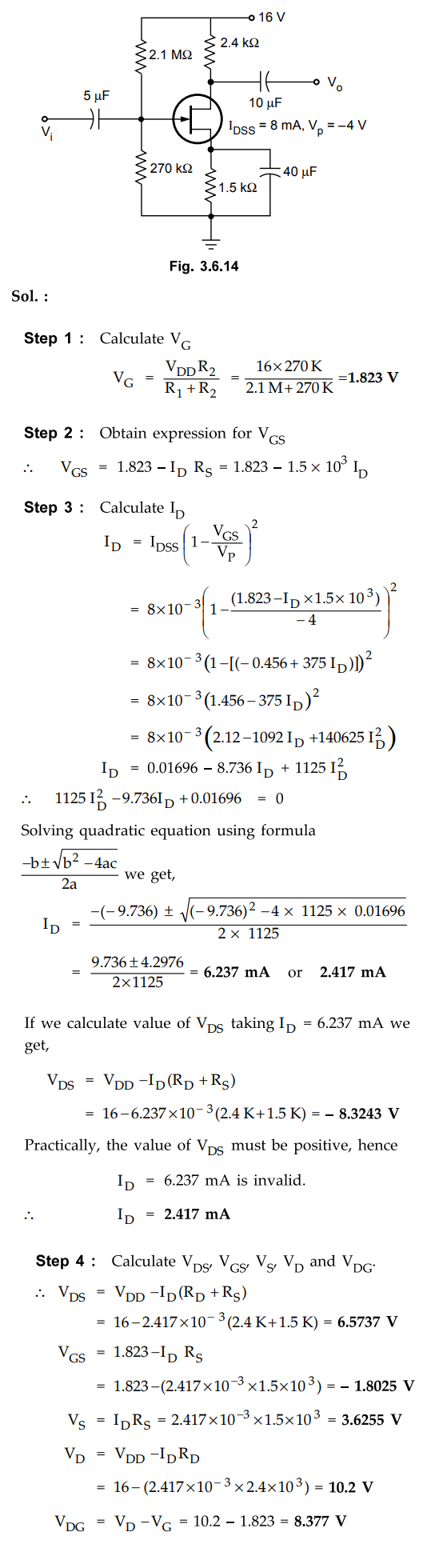
3.6.8 Determine IDQ, VGSQ, VD, V^ VDS and VDG for the network of Fig. 3.6.14.
Ex.
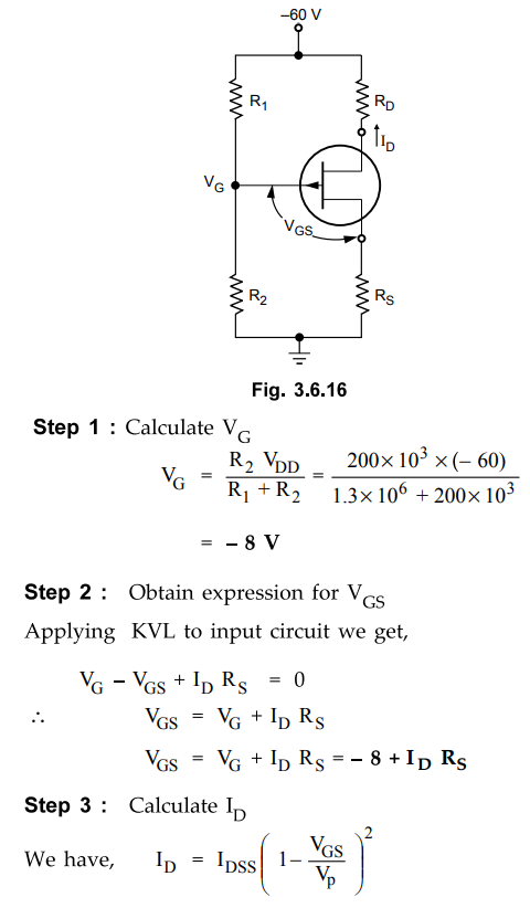
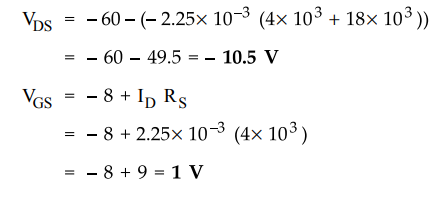
3.6.9 For the circuit shown in Fig. 3.6.15, the FET has Vp = 4 V, IDSS = 4 mA
Calculate
i) IDSQ ii) VGSQ iii) VDSQ

Sol
:
Simplified circuit for d.c. analysis is shown in Fig 3.6.16
Substituting
value of VGS in the above equation and solving for ID we
get,

Practically,
value of VDS for p-channel FET should be negative, hence value of ID
= 4 mA is invalid.
ID
= 2.25 mA
Step
4 : Calculate VDS and VGS
Now
calculating VDS taking ID = 2.25 mA
Example
for Practice
Ex.
3.6.10 : For circuit shown in Fig 3.6.17 Calculate ID , VGS ,
VG , VDS and VS

Review Questions
1. Draw two different
circuits that bias a JFET amplifier.
2. With the help of a
neat diagram explain the voltage divider biasing method for JFET.
3. What are the
different biasing methods of JFET ?
4. Draw the source
self bias and voltage divider bias circuit for FET.
5. Explain the voltage
divider bias circuit for n-channel JFET gives its d.c. analysis.
6. Discuss the source
self-bias and voltage divider bias for FET.
7. Explain about the
common source self bias and voltage divider bias for FET.
8. With the help of
neat diagram, explain methods used in biasing the FET.
Electron Devices and Circuits: Unit II: (b) Junction Field Effect Transistor (JEET) : Tag: : Solved Example Problems | Junction Field Effect Transistor (JFET) - Biasing of JFET
Related Topics
Related Subjects

Electron Devices and Circuits
EC3301 3rd Semester EEE Dept | 2021 Regulation | 3rd Semester EEE Dept 2021 Regulation