Electron Devices and Circuits: Unit II: (c) MOSFET
Biasing of MOSFET
Solved Example Problems
• Common-source circuit is one of the basic MOSFET circuit configurations. The Fig. 4.5.1(a) shows the n-channel enhancement-mode MOSFET circuit with the source terminal is at ground potential and is common to both the input and output sides of the circuit.
Biasing of MOSFET
•
Common-source circuit is one of the basic MOSFET circuit configurations. The
Fig. 4.5.1(a) shows the n-channel enhancement-mode MOSFET circuit with the
source terminal is at ground potential and is common to both the input and
output sides of the circuit.

• It is important to note that the coupling
capacitor Cc acts as an open circuit to d.c. but it allows the signal voltage
to be coupled to the gate of the MOSFET.
•
The d.c. equivalent circuit is shown in Fig. 4.5.1 (b).

•
Since the gate current into the MOSFET is zero, the voltage at the gate is
given by a voltage divider, which can be written as,
•
Assuming that the gate-to-source voltage given by equation (4.5.1) is greater than
VT and MOSFET is biased in the saturation region, the drain current is,
ID
= K(VGS – VT)2 … (4.5.2)
•
Note that, capital notations for voltage and current indicate d.c. values.
•
Applying KVL to drain circuit we have,
VDS
= VDD - ID RD
•
If VDS > VDS(sat) = VGS - VT,
then the MOSFET is biased in the saturation region, as we initially assumed,
and our analysis is correct. If VDS < VDS(sat) then
the MOSFET is biased in the nonsaturation region, and the drain current is
given by,
ID
= K [2(VGS – VT) VDS V2GS ]
Ex.
4.5.1 For the circuit shown in Fig. 4.5.1 (b), assume that R1 = 30 kΩ,
R2 = 10 kΩ, RD = 40 kΩ, VDD = 10 V, VT = 1V VGS
= 2V K = 0.1mA/v2. Find ID
and VDS.
Sol.
:
Step
1 : Calculate VG
From
the circuit shown in Fig. 4.5.2 and equation (4.5.1), we have,
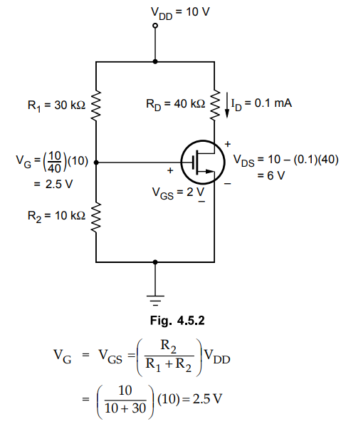
Step
2 : Calculate lD
Assuming
the MOSFET is biased in the saturation region, the drain current is,
ID
= K(VGS –VT)2 = (0.1) (2-1)2
= 0.1mA
Step
3 : Calculate VDS
VDS
= VDD - ID RD = 10 -
(0.1) (40) = 6 V
Validity
of assumption : Because
VDS
= 6 V > VDS(sat) = VGS - VT = 2 - 1 = 1V, the MOSFET
is indeed biased in the saturation region and our calculations are valid.
Ex.
4.5.2 Calculate the D.C. operating condition for the circuit diagram shown in
Fig. 4.5.3.
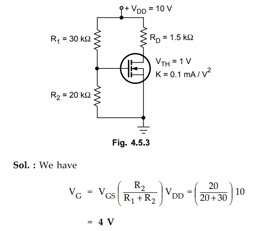
Assuming
transistor is biased in the saturation, the drain current is

Comment
:
Because VDS = 8.65 V > VDS(sat) = VGS
- VT = 4 - 1 = 3, the transistor is indeed biased in the
saturation region and our analysis is valid.
Biasing
circuit for p-channel enhancement-mode MOSFET
•
Fig. 4.5.4 shows a common-source circuit with a p-channel enhancement-mode
MOSFET.
•
Here, the source is tied to +VDD/ which become signal ground in the a.c.
equivalent circuit. Thus it is also a common-source circuit.
•
The d.c. analysis for this circuit is essentially the same as for the n-channel
MOSFET circuit. The gate voltage is given by,
VG
= (R2 / R1 R2)(VDD) ….(4.5.4(a))
and
the source-to-gate voltage is given by,
VSG
= VDD -VG …. (4-5.4 (b))
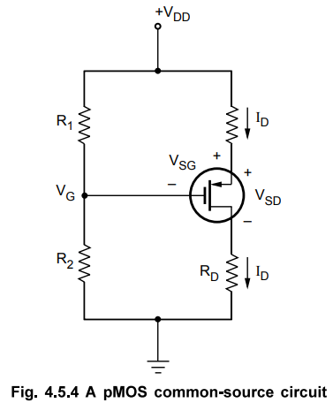
•
Assuming that VGS < VT , or VSG > |VT
|, and that the device is biased in the saturation region, the drain current is
given by,
ID-
K(VSG + VT)2 ...(4.5.5)
and
the source-to-drain voltage is,
VSD
= VDD - IDRD
•
If VSD > VSD(sat) = VSG + VT the MOSFET is indeed biased in the saturation
region, as we have assumed. However, if VSD < VSD(sat)
the MOSFET is biased in the nonsaturation region.
Ex.
4.5.3 Calculate the drain current and source to drain voltage of a common
source circuit, shown in the Fig. 4.5.5. Also verify the region of operation.
Device parameters VT = - 0.8 V and k = 0.2 mAJV2.

Sol.
:

Since
| VGS | > | VT | it is the nonlinear region of
operation.
Ex.
4.5.4 Consider the circuit shown in Fig. 4.5.6. Assume that, R1 = 20 kΩ, R2 =
60 kΩ, VDD = 10 V, RD=15kΩ, VT=-0SV, and K = 0.2 mA/v2. Find ID and
VSD

Sol.
: From the circuit shown in Fig. 4.5.6 we have,

The
source-to-gate voltage is therefore,
VSG
= VDD – VG = 10 -7.5 = 2.5 V
Assuming
the MOSFET is biased in the saturation region, the drain current is,
ID
= K(VSG + VT)2
=
(0.2) (2.5 -0.8)2 = 0.578 mA
and
the source-to-drain voltage is
VSD
= VDD IDRD
=
10 – (0.578) (15) = 1.33 V
•
Since VSD = 1.33 V is not greater than VSD(sat) = VSG
+ VT = 2.5 - 0.8 = 1.7 V, the p-channel MOSFET is not biased in the
saturation region, as we initially assumed.
Calculate
ID for nonsaturation region
•
In the nonsaturation region, the drain current is given by,
ID
= K[2(VSG + VT)VSD –V2SD]
and
the source-to-drain voltage is
VSD
= VSD - ID RD
Combining
these two equation, we obtain
ID
= K[2(VSG + VT)(VDD - IDRD) (VDD - IDRD)2]
For
simplicity, we take resistance values in k Ω so we get value of ID in mA.

•
To bias MOSFET in non-saturation region VSD < VSD(sat)
the VSD = L48 V satisfies this condition and hence ID =
0.568 mA is valid. Thus,
ID
= 0.568 mA and VSD = 1.48 V
1. Load Line and Modes of Operation
•
The load line gives a graphical picture by which we can visualize the region in
which the MOSFET is biased.
•
Consider the common-source circuit shown in Fig. 4.5.7 (a).
•
Writing Kirchhoff's voltage law around the drain-source loop results VDS
= VDD - IDRD, which is the load line equation.
•
It shows a linear relationship between the drain current and drain-to-source
voltage.
•
Fig. 4.5.7 (b) shows the VDS(sat) characteristic for the MOSFET described in
example 4.5.1.
•
The load line is given by
and
is also plotted in the figure. The two end points of the load line are
determine in the usual manner. If the drain current = 0, then VDS= 10 V; VDS
" 0, then drain current = 10/40 = 0.25 mA.
•
The Q-point of the MOSFET is given by the d.c. drain current (ID) and
drain-to-source voltage (VDS) and it is always on the load line, as shown in
the Fig. 4.5.7 (b).
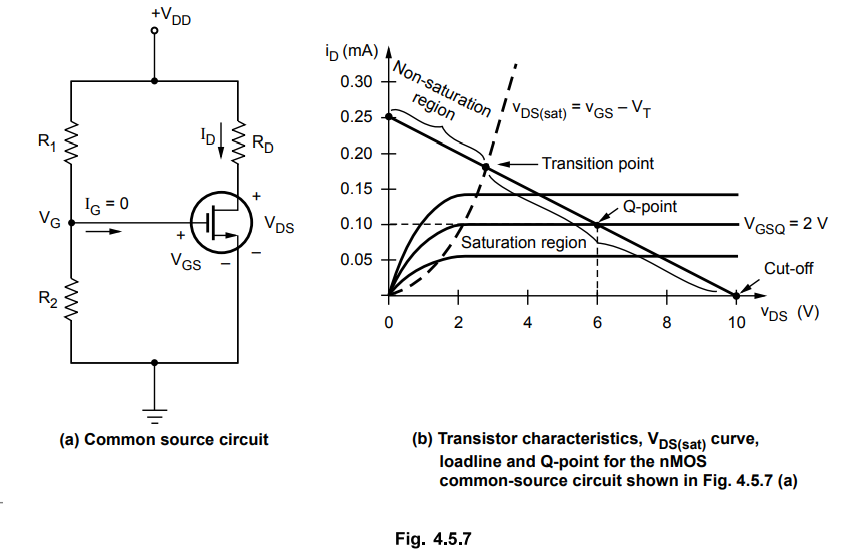
•
If the gate-to-source voltage is less than VT, the drain current is zero and
the MOSFET is in cut-off.
•
As the gate-to-source voltage becomes just greater than the threshold voltage,
the MOSFET turns ON and is biased in the saturation region.
•
As VGS increases, the Q-point moves upon the load line.
•
The transition point is the boundary between the saturation and non-saturation
regions. It is the point where,
•
VDS = VDS(sat) = VGS - VT . AS VGS
increases further, the MOSFET operates in nonsaturation region.
Ex.
4.5.5 Consider the circuit shown in Fig. 4.5.7 (a). Assume VT = 1V
and
K
= 0.1mA/v2. Determine the transition parameters for the given
circuit.
Sol.
:
At the transition point,

•
For VGS < 2.461 V the MOSFET is biased in the saturation region and for VGS
> 2.461 V, the MOSFET is biased in the nonsaturation region.
Summary
of step in the d.c. analysis of MOSFET circuits
•
To analyze the d.c. response of a MOSFET circuit we require to know the bias
condition (saturation or non-saturation) of the MOSFET. In some cases, the bias
condition is not given, which means that we have to assume any one bias
condition, then analyze the circuit to determine if the solution consistent
with our initial assumption. To do this, we have to perform following steps.
1.
Assume that, the MOSFET is biased in the saturation region, in which case VGS
> VT, ID > 0 and VDS ≥ VDs(sat)
2. Analyze the circuit using the saturation
current-voltage relations.
3.
Evaluate the resulting bias condition of the MOSFET. If the assumed parameter
values in step-1 are valid, then the initial assumption is correct. If VGS
< VT, then the MOSFET is probably cut-off, and if VDS <
VDS(sat), the MOSFET is likely biased in the non-saturation region.
4.
If the initial assumption is proved incorrect, then a new assumption must be
made and the circuit must be reanalyzed.
2. Common MOSFET Configurations : D.C. Analysis
•
There are various other MOSFET circuit configurations. Let us analyze and
design them one by one.
a.
CS Circuit with Source Resistor

Voltage
divider bias :
•
Fig. 4.5.9 shows common source circuit with source resistor for n-channel enhancement
type MOSFET.
As
IG = 0A
VG
= R2 VDD / R1 + R2 … (4.5.5)
Applying
KVL to output circuit we get,

Ex.
4.5.6 For the circuit shown in Fig. 4.5.10. Calculate VG, ID,
and VDS.

Sol
:
Step
1 : Calculate VG

Step
2 : Obtain expression for VGS

Step
3 : Calculate K
Step
4 :
Obtain the value of IDQ
Assuming
that the gate to source voltage is greater than VT and transistor is
biased in the saturation region.
We
have, ID = K(VGS
- VT )2
Substituting
value of VGS we get,
Ex.
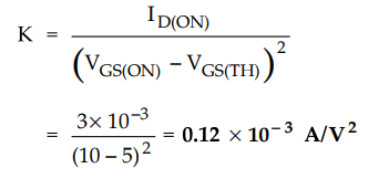
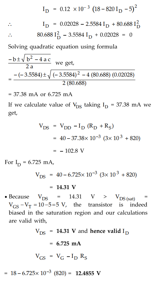
4.5.7 Determine IDQ, VGSQ, VD and VS
for the MOSFET circuit shown in Fig. 4.5.11. Given for MOSFET, VGS(+h) =
3 V, ID(ON) = 5 mA, VGS(ON) = 6 v.

Sol
:

Ex.
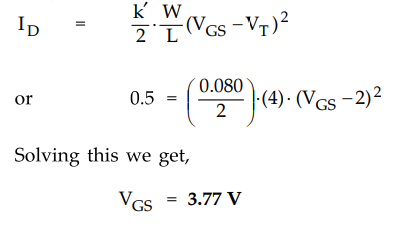
4.5.8 For the d.c. circuit in Fig. 4.5.12 assume the MOSFET parameters are VT
=2 V, k' = 80 µA/V2 and W/L = 4. Choose R1 and R2 such that the current in the
bias resistors is approximately one-tenth of ID. Design the circuit such that
ID = 0.5 mA. Use standard resistor values.

Sol.
:
Assuming the MOSFET is biased saturation region, we have,
The
current through the bias resistor should be approximately

The
closest standard resistor values are R2 =120 kΩ and R1 =
300 kΩ
Validity
of assumption :

Therefore,
the MOSFET is biased in the saturation region, as initially assumed.
Important
Concept
There
are certain tolerances in resistor values as well as tolerances in MOSFET
conduction parameter and threshold voltage values. These tolerances lead to
variations in the Q-point values. Thus, Q-point should not be designed too
close to the transition point to avoid Q-point to enter into nonsaturation
region because of parameter variations. In bipolar circuits, we have seen that
the Q-point tended to be stabilized when an emitter resistor was included in
the circuit. In a similar way, the Q-point of MOSFET circuits will tend to be
stabilized against variations in transistor parameters by including a source
resistor.
Ex.
4.5.9 Determine the d.c. bias point for the EMOSFET circuit in Fig. 4.5.13.
Assume k = 0.4 mA/V2, VT = 3 V.

Sol.
: The
Fig. 4.5.13 (a) shows the equivalent circuit

Ex.
4.5.10 For the E-MOSFET ci rcuit shown in Fig. 4.5.14, VDS = 1/2 VDD
and ID = ID(ON). Determine VDD, RD
and VGS For MOSFET, VGS(ON) = 6V, ID(ON) = 4
mA and VGS(+h) = 3 V.

Electron Devices and Circuits: Unit II: (c) MOSFET : Tag: : Solved Example Problems - Biasing of MOSFET
Related Topics
Related Subjects

Electron Devices and Circuits
EC3301 3rd Semester EEE Dept | 2021 Regulation | 3rd Semester EEE Dept 2021 Regulation