Electron Devices and Circuits: Unit IV: Multistage and Differential Amplifiers
BiCMOS Amplifiers
Equivalent circuit, Solved Example Problems | Multistage Amplifiers
• So far we have seen two basic amplifier technologies, the bipolar technology, which uses npn and pnp bipolar junction transistors, and the MOS technology, which uses NMOS and PMOS field effect transistors.
BiCMOS Amplifiers
•
So far we have seen two basic amplifier technologies, the bipolar technology,
which uses npn and pnp bipolar junction transistors, and the MOS technology,
which uses NMOS and PMOS field effect transistors.
•
An infinite input resistance.
•
A large transconductance due to the bipolar transistor Q2.
•
The bipolar junction transistors have a larger transconductance than MOS
transistors biased at the same current level and they have higher switching
speed. Due to large transconductance they provide larger voltage gains.
•
On the other hand, MOS transistors have an essentially infinite input impedance
at low frequencies and have very high packaging density. Due to almost infinite
input impedance, MOS transistors have zero input bias current.
•
The advantages of these two technologies can be exploited by combining bipolar
and MOS transistors on the same substrate, i.e. in the same integrated circuit.
Such technology is known as BiCMOS technology.
•
We are familiar with the Darlington pair configuration of transistor. Fig. 8.2.1
(a) shows a modified Darlington pair configuration. It uses the bias current
IBIAS/ or some equivalent element to control the quiescent current in
transistor Qr The effective current gain of bipolar transistors is boosted in
this circuit.
•
Fig. 8.2.1 (b) shows a BiCMOS Darlington pair configuration. Here, transistor
Qi is replaced with a MOSFET. This circuit has following advantages.

•
As infinite input resistance
•
A large transconductance due to the bipolar transistor Q2.
Circuit
Analysis
•
Consider the small signal equivalent circuit shown in Fig. 8.2.2.

•
Where gcm is the composite transconductance. The gm2 of
the bipolar transistor is usually at least an order of magnitude greater than
gm1 of the MOSFET. Therefore, the composite transconductance is approximately
an order of magnitude greater than that
of the MOSFET alone. This circuit has following advantages.
•
A large transconductance.
•
An infinite input resistance.
•
Fig. 8.2.3 (a) shows a bipolar cascade circuit, and Fig. 8.2.3 (b) shows a
corresponding BiCMOS configuration.

Bipolar
cascode configuration
•
The output resistance of cascode circuit is very high.
•
The input resistance looking into the emitter of Q2 is very low, thereby
minimizing the Miller multiplication effect. Therefore, the cascode amplifier
has a wider frequency bandwidth than the common-emitter circuit.
BiCMOS
cascode configuration
•
This circuit has the advantage of the infinite input resistance of M1.
•The
frequency response of a BiCMOS cascode circuit is superior to that of an all
MOSFET cascode circuit because the equivalent resistance looking into the
emitter of a bipolar transistor is much less than the resistance looking into
the source of a MOSFET.
2. Current Sources
•
Cascade current sources increase the output resistance and the stability of the
bias current. Fig. 8.2.4 shows a bipolar cascode constant current source.

•
In this circuit, the output resistance is Ro =Pro4. Eventhough, the output
voltage is varied, the bias current remains much more stable than the basic
two-transistor current source.
•
Fig. 8.2.5 shows a BiCMOS double cascode constant current source.

•
The output resistance can be determined from the small signal equivalent
circuit shown in Fig. 8.2.6.

•
In this circuit,
•
The gate voltage to M6 and the base voltage to Q2 and Q4 are constants. It is
equivalent to signal ground.
•
Vπ2 = 0, therefore gm6 Vπ2 = 0.
•
The equivalent circuit can be rearranged as shown in Fig. 8.2.7.
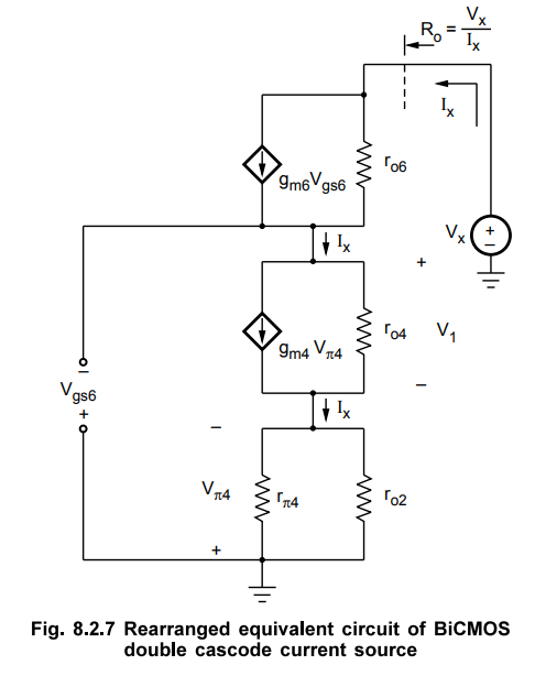
•
For the circuit shown in Fig. 8.2.7.
•
The output resistance is extremely large.
•
The output is given by,
Ro
≅ (gm6ro6)
(β ro4)
•
In this circuit, the output resistance is increased by a factor (gmro6)
compared to the bipolar cascode circuit in Fig. 8.2.4.
• If M6 is to be replaced by a bipolar transistor, then a resistance rn 6 would be connected across the terminals indicated by Vgs6- This resistance would effectively eliminate the multiplying constant gm6ro6, and the output resistance would be essentially the same as that of the circuit shown in Fig. 8.2.4.
3. BiCMOS Differential Amplifier
•
Fig. 8.2.8 shows a basic BiCMOS differential amplifier, with a constant-current
source bias and a bipolar active load.

•
The advantages of this circuit are,
•
The infinite input resistance
•
The zero input bias current.
•
The disadvantage of this circuit is, since the MOSFET is used in the input
stage, the offset voltage is relatively high compared to that of a bipolar
input circuit. The offset voltages are generated because of the mismatching of
differential pair input transistors.
4. BiCMOS Inverter
•
The Fig. 8.2.9 shows the BiCMOS circuit. It consists of two bipolar transistors
(T3 and T4), one nMOS and one pMOS transistor (both enhancement-type devices,
OFF at Vin = 0 V).

•
In this circuit the MOS switches perform the logic function and bipolar
transistors drive output loads.
When
Vin = 0 :
T1
is OFF , therefore T3 is non-conducting.
T2
is ON and supplies current to base of T4
T4
base voltage is set to Vdd.
•
T4 conducts and acts as current source to charge load CL towards Vdd.
Vout rises to Vdd – Vbe (of T4)
where Vbe (of T4) is base emitter voltage of T4. It is
important to note that the pullup bipolar transistor T4 turns off as the output
approaches 5V - Vbe (ofT4)
When
Vin = Vdd
T2
is OFF therefore T4 is non-conducting.
T1
is ON and supplies current to the base of T3.
•
T3 conducts and acts as a current sink to discharge load CL towards
0 V.
Vout
falls to 0 V + VCE(sat) (of T3). The VCE(sat) (of
T,) is saturation voltage from T3 collector to emitter.
•
The T3 and T4 present low impedances when turned ON into
saturation and load CL will be charged or discharged rapidly.
•
The output logic levels will be good and will be close to rail voltages since
VCE(sat) is quite small and VBE ≈ 0.7 V. Therefore, inverter has
high noise margins.
•
Such inverter has high input impedance and low output impedance.
•
The inverter also has high drive capability but occupies a relatively small
area.
Review Questions
1. Describe the BiCMOS circuits of MOSFET.
2. Explain with neat diagram BiCMOS inverter.
3. Draw and explain the BiCMOS cascode amplifier.
4. Draw and explain the basic BiCMOS differential amplifier.
Electron Devices and Circuits: Unit IV: Multistage and Differential Amplifiers : Tag: : Equivalent circuit, Solved Example Problems | Multistage Amplifiers - BiCMOS Amplifiers
Related Topics
Related Subjects

Electron Devices and Circuits
EC3301 3rd Semester EEE Dept | 2021 Regulation | 3rd Semester EEE Dept 2021 Regulation