Microprocessors and Microcontrollers: Unit IV: (c) Programmable Interval Timer (PIT/C) 8253/8254
Block Diagram
Review Questions 1. Draw and explain the functional block diagram of 8253/54 timer. 2. Discuss the internal architecture of 8253 programmable interval timer. 3. Explain the block diagram of the 8254 timer. 4. Draw and explain the functional block diagram of 8254 timer.
Block Diagram
Fig.
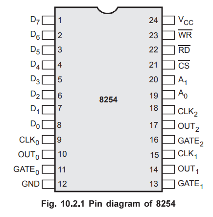
10.2.1 and Fig. 10.2.2 show the pin diagram and block diagram of 8253/54. The
block diagram of 8253/54 includes three counters, a data bus buffer, Read/Write
control logic, and a control register. Each counter has two input signals CLOCK
and GATE and one output signal OUT.
Data
Bus Buffer : This tri-state, bi-directional, 8-bit
buffer is used to interface the 8253/54 to the system data bus. The Data bus
buffer has three basic functions.
1.
Programming the 8253/54 in various modes.
2.
Loading the count registers.
3.
Reading the count values.
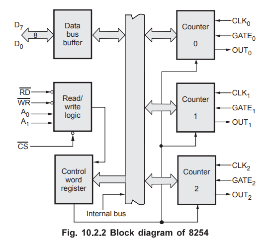
Read/Write
Logic : The Read/Write logic has five signals :  and the address lines A0 and A1. In the peripheral I/O
mode, the
and the address lines A0 and A1. In the peripheral I/O
mode, the ![]() , and
, and ![]() signals are connected to
signals are connected to  ,
respectively. In memory-mapped I/O, these are connected to
,
respectively. In memory-mapped I/O, these are connected to  . Address
lines A0 and A1 of the CPU are usually connected to lines
A0 and A1 of the 8253/54, and
. Address
lines A0 and A1 of the CPU are usually connected to lines
A0 and A1 of the 8253/54, and ![]() is tied to a
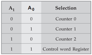
decoded address. The control word register and counters are selected according
to the signals on lines A0 and A1
is tied to a
decoded address. The control word register and counters are selected according
to the signals on lines A0 and A1
Control
Word Register : This register is accessed when lines A0
and A1 are at logic 1. It is used to write a command word which
specifies the counter to be used (binary or BCD), its mode and either a read or
write operation.
Counters
:
These three functional blocks are identical in operation. Each counter consists
of a single, 16 bit, pre-settable, down counter. The counter can operate in
either binary or BCD and its input, gate and output are configured by the
selection of modes stored in the control word register. The counters are fully
independent. The programmer can read the contents of any of the three counters
without disturbing the actual count in process.
Review Questions
1. Draw and explain
the functional block diagram of 8253/54 timer. AU : May-13, Marks 8
2. Discuss the
internal architecture of 8253 programmable interval timer. AU : May-14, Marks 16
3. Explain the block
diagram of the 8254 timer. AU : Dec.-15, Marks 4
4. Draw and explain the functional block diagram of 8254 timer. AU : May-16, Marks 8
Microprocessors and Microcontrollers: Unit IV: (c) Programmable Interval Timer (PIT/C) 8253/8254 : Tag: : - Block Diagram