Microprocessors and Microcontrollers: Unit IV: (d) Serial Data Transfer (USART) 8251
Block Diagram
Serial Data Transfer (USART) 8251
Fig. 12.4.1 shows the block diagram of IC 8251A. It includes: Data bus buffer, Read/Write control logic, Modem control, Transmit buffer, Transmit control, Receiver buffer and Receiver control.
Block Diagram
Fig.
11.4.1 shows the block diagram of IC 8251A. It includes: Data bus buffer,
Read/Write control logic, Modem control, Transmit buffer, Transmit control,
Receiver buffer and Receiver control.

Data
Bus Buffer: This tri-state, bi-directional, 8-bit
buffer is used to interface 8251 to the system data bus. Along with the data,
control word, command words and status information are also transferred through
the data bus buffer.
Read/Write Control Logic : This functional block accepts inputs from the system control bus and generates control signals for overall device operation. It decodes control signals on the 8085 control bus into signals which controls the internal and external I/O bus. It contains the control word register and command word register that stores the various control formats for the device functional definition.
Transmit
Buffer : The transmit buffer accepts parallel data from the
CPU, adds the appropriate framing information, serializes it, and transmits it
on the TxD pin on the falling edge of ![]()
It
has two registers : A buffer register to hold eight bits and an output register
to convert eight bits into a stream of serial bits. The CPU writes a byte in
the buffer register, which is transferred to the output register when it is
empty. The output register then transmits serial data on the TxD pin.
In
the asynchronous mode the transmitter always adds START bit; depending on how
the unit is programmed, it also adds an optional even or odd parity bit, and
either 1, 1 ½ , or 2 STOP bits. In
synchronous mode no extra bits (other than parity, if enable) are generated by
the transmitter.
Transmit
control
It
manages all activities associated with the transmission of serial data. It
accepts and issues signals both externally and internally to accomplish this
function.
TxRDY
(Transmit Ready ) : This output signal indicates CPU that
buffer register is empty and the USART is ready to accept a data character. It
can be used as an interrupt to the system or, for polled operation, the CPU can
check TxRDY using the status read operation. This signal is reset when a data
byte is loaded into the buffer register.
TxE
(Transmitter Empty) : This is an output signal. A high on
this line indicates that the output buffer is empty. In the synchronous mode,
if the CPU has failed to load a new character in time, TxE will go high
momentarily as SYNC characters are loaded into the transmitter to fill the gap
in transmission.
![]() (Transmitter Clock) : This clock controls the rate at which
characters are transmitted by USART. In the synchronous mode
(Transmitter Clock) : This clock controls the rate at which
characters are transmitted by USART. In the synchronous mode ![]() is
equivalent to the baud rate, and is supplied by the modem. In asynchronous mode
is
equivalent to the baud rate, and is supplied by the modem. In asynchronous mode ![]() is 1, 16, or 64 times the baud rate. The clock division is
programmable. It can be programmed by writing proper mode word in the mode set
register.
is 1, 16, or 64 times the baud rate. The clock division is
programmable. It can be programmed by writing proper mode word in the mode set
register.
Receiver
Buffer : The receiver accepts serial data on the RxD line,
converts this serial data to parallel format, checks for bits or characters
that are unique to the communication technique and sends an
"assembled" character to the CPU.
When
8251A is in the asynchronous mode and it is ready to accept a character, it
looks for a low level on the RxD line. When it receives the low level, it
assumes that it is a START bit and enables an internal counter. At a count
equivalent to one-half of a bit time, the RxD line is sampled again. If the
line is still low, a valid START bit is detected and the 8251A proceeds to
assemble the character. After successful reception of a START bit the 8251A
receives data, parity and STOP bits, and then transfers the data on the
receiver input register. The data is then transferred into the receiver buffer
register.
In
the synchronous mode the receiver simply receives the specified number of data
bits and transfers them to the receiver input register and then to the receiver
buffer register.
Receiver
Control : It manages all receiver-related activities. Along
with data reception, it does false start bit detection, parity error detection,
framing error detection, sync detection and break detection.
RxRDY
(Receiver Ready) : This is an output signal. It goes high
(active), when the USART has a character in the buffer register and is ready to
transfer it to the CPU. This line can be used either to indicate the status in
the status register or to interrupt the CPU. This signal is reset when a data
byte from receiver buffer is read by the CPU.
![]() (Receiver Clock) : This clock controls the rate at which
the character is to be received by USART in the synchronous mode.
(Receiver Clock) : This clock controls the rate at which
the character is to be received by USART in the synchronous mode. ![]() is
equivalent to the baud rate, and is supplied by the modem. In asynchronous mode
is
equivalent to the baud rate, and is supplied by the modem. In asynchronous mode ![]() is 1, 16, or 64 times the baud rate. The clock division is
programmable. It can be programmed by writing proper mode word in the mode set
register.
is 1, 16, or 64 times the baud rate. The clock division is
programmable. It can be programmed by writing proper mode word in the mode set
register.
Modem
Control : The 8251 has a set of control inputs and outputs
that can be used to simplify the interface to almost any modem. It provides
control circuitry for the generation of 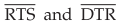 and the reception of
 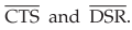 In addition, a general purpose inverted output and a general purpose input are
provided. The output is labeled
In addition, a general purpose inverted output and a general purpose input are
provided. The output is labeled ![]() and the input is labeled
and the input is labeled  can be asserted by setting bit 2 of the command instruction; DSR can be sensed
as bit 7 of the status register. When used as a modem control signal
can be asserted by setting bit 2 of the command instruction; DSR can be sensed
as bit 7 of the status register. When used as a modem control signal ![]() indicates that the terminal is ready to communicate and
indicates that the terminal is ready to communicate and ![]() indicates that it
is ready for communication.
indicates that it
is ready for communication.
Review
Questions
1.
With neat block diagram, explain the architecture of 8251 USART. AU : Dec.-07,
May-08,11, Marks 16
2.
Draw and explain the functional block diagram of 8251 USART.
AU : May-13, Marks 16
3.
With functional block diagram, explain the operation and programming
AU : May-11, Marks 16
4.
Draw and explain the functional block diagram qf 8251. AU : May-13, Marks 8 AU : May-16, Marks 8
Microprocessors and Microcontrollers: Unit IV: (d) Serial Data Transfer (USART) 8251 : Tag: : Serial Data Transfer (USART) 8251 - Block Diagram