Microprocessors and Microcontrollers: Unit IV: (b) Programmable Interrupt Controller (PIC) - 8259
Block Diagram of 8259A
Programmable Interrupt Controller (PIC) - 8259
Fig. 9.3.1 shows the internal block diagram of the 8259A. It includes eight blocks: data bus buffer, read/write logic, control logic, three registers (IRR, ISR and IMR), priority resolver, and cascade buffer.
Block Diagram of 8259A
Fig.
9.3.1 shows the internal block diagram of the 8259A. It includes eight blocks:
data bus buffer, read/write logic, control logic, three registers (IRR, ISR and
IMR), priority resolver, and cascade buffer.

Data
Bus Buffer : The data bus buffer allows the 8085 to
send control words to the 8259A and read a status word from the 8259A. The
8-bit data bus buffer also allows the 8259A to send interrupt opcode and
address of the interrupt service subroutine to the 8085.
Read/Write Logic :
The 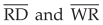 inputs control the data flow on the data bus when the device is
selected by asserting its chip select
inputs control the data flow on the data bus when the device is
selected by asserting its chip select ![]() input low.
input low.
Control
Logic : This block has an input and an output line. If the
8259A is properly enabled, the interrupt request will cause the 8259A to assert
its INT output pin high. If this pin is connected to the INTR pin of an 8085
and if the 8085 Interrupt Enable (IE) flag is set, then this high signal will
cause the 8085 to respond INTR as explained earlier.
Interrupt
Request Register (IRR) : The IRR is used to store all the
interrupt levels which are requesting the service. The eight interrupt inputs
set corresponding bits of the Interrupt Request Register upon service request.
Interrupt
Service Register (ISR) : The Interrupt Service Register
(ISR) stores all the levels that are currently being serviced.
Interrupt
Mask Register (IMR) : Interrupt Mask Register (IMR) stores
the masking bits of the interrupt lines to be masked. This register can be
programmed by an Operation Command Word (OCW). An interrupt which is masked by
software will not be recognised and serviced even if it sets the corresponding
bits in the IRR.
Priority
Resolver (PR) : The priority resolver determines the
priorities of the bits set in the IRR. The bit corresponding to the highest
priority interrupt input is set in the ISR during the  input.
Cascade
Buffer Comparator : This section generates control signals
necessary for cascade operations. It also generates Buffer-Enable signals. As
stated earlier, the 8259 can be cascaded with other 8259s in order to expand
the interrupt handling capacity to sixty-four levels. In such a case, the
former is called a master, and the latter are called slaves. The 8259 can be
set up as a master or a slave by the  pin.
pin.
CAS0
- CAS2 : For a master 8259, the CAS0-CAS2
pins are output pins, and for slave 8259s, these are input pins. When the 8259
is a master (that is, when it accepts interrupt requests from other 8259s), the
CALL opcode is generated by the master in response to the first . The
vector address must be released by the slave 8259. The master sends an
identification code of three-bits to select one out of the eight possible slave
8259s on the CAS0 - CAS2 lines. The slave 8259s accept
these three signals as inputs (on their CAS0 - CAS2 pins)
and compare the code sent by the master with the codes assigned to them during
initialisation. The slave thus selected (which had originally placed an
interrupt request to the master 8259) then puts the address of the interrupt
service routine during the second and third pulses from the MPU.
 (Slave Program I Enable Buffer) : The
  signal is tied high for the master. However it
is grounded for the slave.
signal is tied high for the master. However it
is grounded for the slave.
In
large systems where buffers are used to drive the data bus, the data sent by
the 8259 in response to cannot be accessed by the MPU (due to the
data bus buffer being disabled). If an 8259 is used in the buffered mode
(buffered or non-buffered modes of operation can be specified at the time of
initialising the 8259), the in
is used as an output which can be used to enable the system data bus buffer
whenever the data bus outputs of 8259 are enabled (i.e. when it is ready to
send data).
Thus,
in non-buffered mode, the ppin of an 8259 is used to specify
whether the 8259 is to operate as a master or as a slave, and in the buffered
mode, the in is used as an output to enable the data bus buffer
of the system.
Review Questions
1. With a neat
diagram, discuss the functional organization of a programmable interrupt
controller. AU : Dec.-09,11 Marks 16
2. State the use of
ISR and PR registers in 8259 PIC. AU : Dec.-11, Marks 2
3. List the major
components of 8259 A interrupt controller and explain their functions. AU : Dec -12, Marks 8
4. Explain the working
of 8259 with a neat block diagram. AU : Dec.-16, 19, Marks 8
5. Explain the
architecture of 8259. AU : Dec -18, Marks
9
Microprocessors and Microcontrollers: Unit IV: (b) Programmable Interrupt Controller (PIC) - 8259 : Tag: : Programmable Interrupt Controller (PIC) - 8259 - Block Diagram of 8259A