Electron Devices and Circuits: Unit V: (a) Feedback Amplifiers
Block Diagram of Feedback Amplifiers
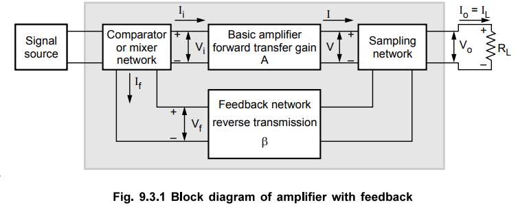
• In feedback amplifier, we sample the output voltage or current by means of a suitable sampling network and apply this signal to the input through a feedback two port network, as shown in the Fig. 9.3.1.
Block Diagram
•
In feedback amplifier, we sample the output voltage or current by means of a
suitable sampling network and apply this signal to the input through a feedback
two port network, as shown in the Fig. 9.3.1.
•
At the input the feedback signal is combined with the input signal through a
mixer network and is fed into the amplifier.
•
As shown in the Fig. 9.3.1 feedback connection has three networks :
•
Sampling Network
•
Feedback Network
•
Mixer Network
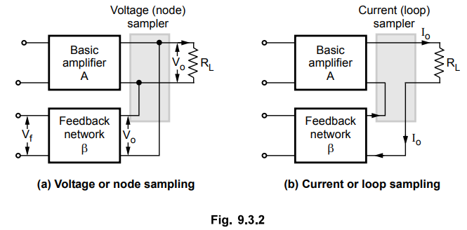
1. Sampling Network
•
There are two ways to sample the output, according to the sampling parameter,
either voltage or current.
•
The output voltage is sampled by connecting the feedback network in shunt
across the output, as shown in the Fig. 9.3.2 (a). This type of connection is
referred to as voltage, or node, sampling.
•
The output current is sampled by connecting the feedback network in series with
the output as shown in the Fig. 9.3.2 (b). This type of connection is referred
to as current, or loop, sampling.
2. Feedback Network
•
It may consists of resistors, capacitors, and inductors. Most often it is
simply a resistive configuration.
•
It provides reduced portion of the output as feedback signal to the input mixer
network. It is given as Vf = P Vo where P is a feedback factor or feedback
ratio.
•
The symbol P used in feedback circuits represents feedback factor which always
lies between 0 and 1. It is totally different from P symbol used to represent
current gain in common emitter amplifier, which is greater than 1.
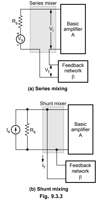
3. Mixer Network
•
Like sampling, there are two ways of mixing feedback signal with the input
signal. These are : series input connection and shunt input connection.
•
The Fig. 9.3.3 (a) and (b) show the simple and very common series (loop) input
and shunt (node) input connections, respectively.
4. Transfer Ratio or Gain
•
In Fig. 9.3.1, the ratio of the output signal to the input signal of the basic
amplifier is represented by the symbol A. The suffix of A given next,
represents the different transfer ratios.
V
/ Vi = Av = Voltage gain … (9.3.1)
I
/ Ii = Ai = Current gain … (9.3.2)
I
/ Vi = Gm = Transconductance… (9.3.3)
V
/ Ii = Rm = Transresistance… (9.3.4)
•
The four quantities Av, Ai ,Gm and Rm are
referred to as a transfer gain of the basic amplifier without feedback and use
of only symbol A represent any one of these quantities.
5. Transfer Ratio or Gain with Feedback
•
The transfer gain with feedback is represented by the symbol Af. It is defined
as the ratio of the output signal to the input signal of the amplifier
configuration shown in Fig. 9.3.1. Hence Af is used to represent any one of the
following four ratios :
Vo
/ Vs = AVf = Voltage gain with feedback ... (9.3.5)
Io
/ Is = AIf Current gain with feedback ... (9.3.6)
Io
/ Io = GMf = Transconductance with feedback ... (9.3.7)
Vo
/ IS = RMf Transresistance
with feedback ... (9.3.8)
•
Fig. 9.3.4 shows the schematic representation of a feedback connection around a
basic amplifier. Recall that, when part of output signal and input signal are
in out of phase the feedback is called negative feedback.

•
The schematic diagram shown in Fig. 9.3.4 represents negative feedback because
the feedback signal is fed back to the input of the amplifier out of phase with
input signal of the amplifier.
Review Questions
1. Give the block diagram of feedback amplifier.
AU : ECE : Dec.-06, Hay-11, Harks 5
2. Explain sampling network.
3. Explain feedback network.
4. Explain mixer network.
5. Define transfer ratio.
6. Draw the block diagram of feedback amplifier and discuss the
effect of negative feedback with respect to closed loop gain, bandwidth and
distortion.
AU : ECE : Dec.-ll, Marks 10
Electron Devices and Circuits: Unit V: (a) Feedback Amplifiers : Tag: : - Block Diagram of Feedback Amplifiers
Related Topics
Related Subjects

Electron Devices and Circuits
EC3301 3rd Semester EEE Dept | 2021 Regulation | 3rd Semester EEE Dept 2021 Regulation