Linear Integrated Circuits: Unit II: Characteristics of Op-amp
Block Diagram Representation of Op-amp
As mentioned earlier, now a days op-amps are available in an integrated circuit form. Commercial integrated circuit op-amps usually consists of four cascaded blocks. The block diagram of IC op-amp is shown in the Fig. 2.3.1.
Block Diagram Representation of Op-amp
As
mentioned earlier, now a days op-amps are available in an integrated circuit
form. Commercial integrated circuit op-amps usually consists of four cascaded
blocks. The block diagram of IC op-amp is shown in the Fig. 2.3.1.
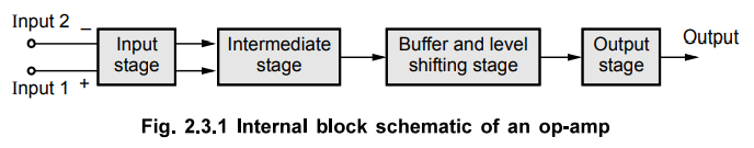
1. Input Stage
The
input stage requires high input impedance to avoid loading on the sources. It
requires two input terminals. It also requires low output impedance. All such
requirements are achieved by using the dual input, balanced output differential
amplifier as the input stage. The function of a differential amplifier is to
amplify the difference between the two input signals. The differential
amplifier has high input impedance. This stage provides most of the voltage
gain of the amplifier.
2. Intermediate Stage
The
output of the input stage drives the next stage which is an intermediate stage.
This is another differential amplifier with dual input, imbalanced i.e. single
ended output. The overall gain requirement of the op-amp is very high. The
input stage alone cannot provide such a high gain. The main function of the
intermediate stage is to provide an additional voltage gain required.
Practically, the intermediate stage is not a single amplifier but the chain of
cascaded amplifiers called multistage amplifiers.
3. Level Shifting Stage
All
the stages are directly coupled to each other. As the op-amp amplifies d.c.
signals also, the coupling capacitors are not used to cascade the stages. Hence
the d.c. quiescent
voltage
level of previous stage gets applied as the input to the next stage. Hence
stage by stage d.c. level increases well above ground potential. Such a high
d.c. voltage level may drive the transistors into saturation. This further may
cause distortion in the output due to clipping. This may limit the maximum a.c.
output voltage swing without any distortion. Hence before the output stage, it
is necessary to bring such a high d.c. voltage level to zero volts with respect
to ground.
The
level shifter stage brings the d.c. level down to ground potential, when no
signal is applied at the input terminals. Then the signal is given to the last
stage which is the output stage.
The
buffer is usually an emitter follower whose input impedance is very high. This
prevents loading of the high gain stage.
4. Output Stage
The
basic requirements of an output stage are low output impedance, large a.c.
output voltage swing and high current sourcing and sinking capability.
The push-pull complementary amplifier meets all these requirements and hence used as an output stage. This stage increases the output voltage swing and keeps the voltage swing symmetrical with respect to ground. The stage raises the current supplying capability of the op-amp.
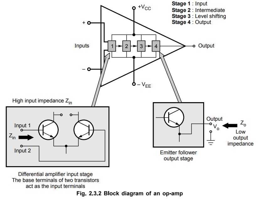
In
short, the overall block diagram can be shown as in the Fig. 2.3.2.
Review Questions
1. Draw the schematic block diagram of the basic op-amp and
briefly explain each stage.
Dec.-06, Marks 8
2. Explain the functions of all the building blocks of an op-amp.
Linear Integrated Circuits: Unit II: Characteristics of Op-amp : Tag: : - Block Diagram Representation of Op-amp
Related Topics
Related Subjects

Linear Integrated Circuits
EE3402 Lic Operational Amplifiers 4th Semester EEE Dept | 2021 Regulation | 4th Semester EEE Dept 2021 Regulation