Electron Devices and Circuits: Unit I: PN Junction Devices
Bridge Rectifier
Circuit Diagram, Operations, Calculation, Formula, Advantages, Disadvantages, Applications, Solved Example Problem
• The bridge rectifier circuit is essentially a full-wave rectifier circuit, using four diodes, forming the four arms of an electrical bridge.
Bridge Rectifier
AU
: May-10,14,17,Dec.-ll,14,17,18
•
The bridge rectifier circuits are mainly used as,
a)
A power rectifier circuit for converting a.c. power to d.c. power, and
b)
A rectifying system in rectifier type a.c. meters, such as a.c. voltmeter, in
which the a.c. voltage under measurement is first converted into d.c. and
measured with conventional meter. In this system, the rectifying elements are
either copper oxide type or selenium type.
•
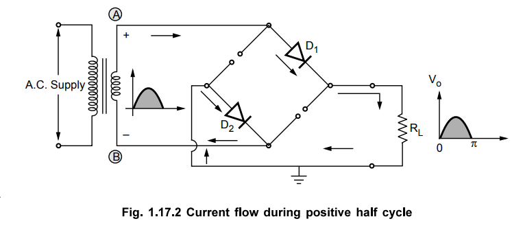
The basic bridge rectifier circuit is shown in Fig. 1.17.1.

•
The bridge rectifier circuit is essentially a full-wave rectifier circuit,
using four diodes, forming the four arms of an electrical bridge. To one
diagonal of the bridge, the a.c. voltage is applied through a transformer if
necessary, and the rectified d.c. voltage is taken from the other diagonal of
the bridge. The main advantage of this circuit is that it does not require a
centre tap on the secondary winding of the transformer. Hence wherever
possible, a.c. voltage can be directly applied to the bridge.
1. Operation of the Circuit
•
Consider the positive half of ac input voltage. The point A of secondary
becomes positive. The diodes D1 and D2 will be forward
biased, while D3 and D4 reverse biased. The two diodes D4
and D2 conduct in series with the load and the current flows
as shown in Fig. 1.17.2.
•
In the next half cycle, when the polarity of ac voltage reverses hence point B
becomes positive diodes D3 and D4 are forward biased, while D4 and D2 reverse
biased. Now the diodes D3 and D4 conduct is series with the load and the
current flows as shown in Fig. 1.17.3.

Key
Point : It is seen that in both cycles of a.c.,
the load current is flowing in the same direction hence, we get a full-wave
rectified output.
•
The waveforms of load current and voltage remain exactly same as shown before
for full-wave rectifier.
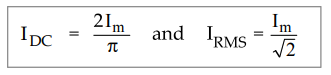
2. Expressions for Various Parameters
•
The bridge rectifier circuit, being basically a full wave rectifier circuit;
all the characteristic discussed previously for a full-wave circuit using two
diodes, are the characteristic of a bridge rectifier circuit.
•
The relation between Im the maximum value of load current and IDC,IRMS
remains same as derived earlier for the full wave rectifier circuit.
•
The expression for I will change slightly. This will be clear from the
equivalent circuit shown in the Fig. 1.17.4.
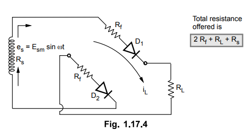
•
In each half cycle two diodes conduct simultaneously. Hence maximum value of
load current is,

Key
Point : So the only modification is that instead of Rp
which is forward resistance of each diode, the term 2Rf appears in the
denominator.
•
The remaining expressions are identical to those derived for two diode full
wave rectifier and reproduced for the convenience of the reader.
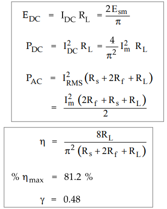
Key
Point : The Esm is the maximum value of a.c.
voltage across full secondary winding of the transformer used.
•
As the current flows through the entire secondary of the transformer for all
the time, the transformer utilization factor is 0.812. This is more than the
T.U.F for full wave rectifier circuit.
3. PIV Rating of Diodes
•
The reverse voltage appearing across the reverse biased diodes is 2Esm
but two diodes are sharing it.
Hence
PIV rating of the is Eam and not 2Eam as in case of full
wave rectifier.
4. What Happens if Input and Output Terminals are Reversed ?
•
The bridge rectifier can be represented in a simplified way as shown in the
Fig. 1.17.5.

•
For positive half cycle of input D1, D2 conduct while for
negative half cycle D3, D4 conduct.
•
It can be noted that if input and output terminals in bridge rectifier are
reversed without any change in diodes then it will not work. For one cycle,
supply will get shorted through the forward biased diodes across the supply
while for other cycle the circuit will be open. The output will be zero.
5. Advantages of Bridge Rectifier Circuit
1)
The current in both the primary and secondary of the power transformer flows
for the entire cycle and hence for a given power output, power transformer of a
small size and less cost may be used.
2)
No centre tap is required in the transformer secondary. Hence, wherever
possible, ac voltage can directly be applied to the bridge.
3)
The current in the secondary of the transformer is in opposite direction in two
half cycles. Hence net d.c. component flowing is zero which reduces the losses
and danger of saturation.
4)
Due to pure alternating current in secondary of transformer, the transformer
gets utilized effectively and hence the circuit is suitable for applications
where large powers are required.
5)
As two diodes conduct in series in each half cycle, inverse voltage appearing
across diodes get shared. Hence the circuit can be used for high voltage
applications. Such a peak reverse voltage appearing across diode is called peak
inverse voltage rating (PIV) of diode.
6. Disadvantages of Bridge Rectifier
•
The only disadvantage of bridge rectifier is the use of four diodes as compared
to two diodes in normal full wave rectifier. This causes additional voltage
drop as indicated by term 2Rf present in expression of Im instead of
Rf . This reduces the output voltage.
7. Applications
1.
Used as rectifier in power circuits to convert a.c. to
2.
In rectifier type meters, to convert a.c. voltage to be measured to d.c.
3.
In power supply circuits.
8. Comparison with Two Diode Rectifier

Ex.
1.17.1 The four semiconductor diodes used in a bridge rectifier circuit each
having a forward resistance of 0.1 Q and infinite reverse resistance, feed a
d.c. current of 10 A to a resistive load from a sinusoidally varying
alternating supply of 30 V (r.m.s). Determine the resistance of the load and
the efficiency of the circuit.
Sol.
:
The given values are,

Ex.
1.17.2 In a bridge rectifier circuit, input supply is 230 V, 50 Hz. Primary to
secondary turns ratio is 4:1, load resistance is 200 Ω. The diodes are ideal.
Find dc output voltage, PIV and output signal frequency.
AU
: Dec-18, Marks 7
Sol.
:

Review Questions
1. Draw the circuit
diagram and explain of full wave bridge rectifier and expression for average
output current, efficiency, peak inverse voltage, TUF factor. the working
derive the rectification and ripple
AU : May-10,14,17,
Dec.-ll,14,18, Marks 8
2. Draw the circuit
diagram and explain of full wave bridge rectifier and expression of average
output current factor. the working derive the and ripple
AU : May-17, Marks 13
3. Explain the working
of a bridge rectifier circuit. Discuss its advantages over centre-tap full wave
rectifier circuit.
4. The four
semiconductor diodes used in a bridge rectifier circuit, each having a forward
resistance of 0.05 Ω and infinite reverse resistance, feed a mean current of 10
A to a resistive load from a sinusoidally varying alternating supply of 30 V
(r.m.s.). Determine the resistance of the load and the efficiency of the
circuit.
(Ans.: RL = 2 Q, %
Efficiency = 78 %)
5. If the required
output d.c. voltage is 9 volts and the voltage drop across each diode is 0.8,
calculate the a.c. r.m.s. input voltage required in the following cases :
i) Bridge rectifier
ii) Centre tap full-wave rectifier.
(V rms =
11.7736 V, Vrms = 10.88 V)
Electron Devices and Circuits: Unit I: PN Junction Devices : Tag: : Circuit Diagram, Operations, Calculation, Formula, Advantages, Disadvantages, Applications, Solved Example Problem - Bridge Rectifier
Related Topics
Related Subjects

Electron Devices and Circuits
EC3301 3rd Semester EEE Dept | 2021 Regulation | 3rd Semester EEE Dept 2021 Regulation