Microprocessors and Microcontrollers: Unit I: (a) 8085 Processor
Bus Organization
Clock Circuit - Demultiplexing AD7 – AD0 - Reset Circuit - Typical Configuration
Questions : 1. Draw the schematic of latching low-order address bus in 8085 microprocessor. 2. Why AD0 – AD7 lines are multiplexed? 3. Draw and explain typical 8085 configuration. 4. Write a note on bus drivers.
Bus Organization
AU : Dec.-11
In
this section we are going to see how we can use various buses of 8085, how to
demultiplex address and data bus, how to generate control signals, how to
provide clock and reset signals to 8085 and so on.
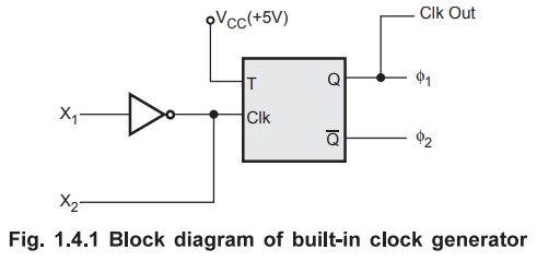
1. Clock Circuit
The
8085 has on chip clock generator. Fig. 1.4.1 shows the internal block diagram
of the on chip clock generator. The internal clock generator requires timed
circuit like LC, RC or crystal, or external clock source as an input to
generate the clock. The internal T-flip flop divides the frequency by 2. Hence
the operating frequency of the 8085 is always half of the oscillator frequency.
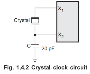
Crystal
Oscillator Circuit : Fig. 1.4.2 shows the crystal oscillator
circuit. It is the most stable circuit. The 20 pF capacitor in the circuit is
connected to assure oscillator start-up at the correct frequency.
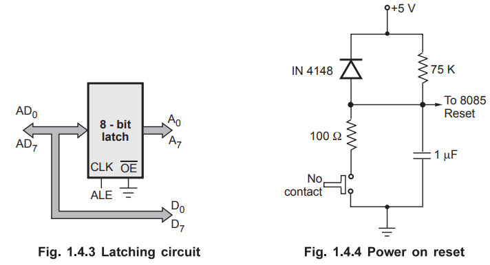
2. Demultiplexing AD7 – AD0
The
latching of lower half of an address is done by using external latch and ALE
signal from 8085. The Fig. 1.4.3 shows the hardware connection for latching the
lower half of an address. The IC 74LS373 is an 8-bit latch, having 8 D flip-flops.
The input is transferred to the output only when clock is high. This clock
signal is driven by ALE signal from 8085. The ALE signal is activated only
during Tlz so input is transferred to the output only during Tx i.e. address (A0
- A7) on the AD0 to AD7 multiplexed bus. In
the remaining part of the machine cycle, ALE signal is disabled so output of
the latch (A0 - A7) remains unchanged. To latch lower
half of an address, in each machine cycle, the 8085 gives ALE signal high
during T1 of every machine cycle. With this circuit, we can use
output of latch as lower half address bus and input of latch (AD0 - AD7)
as data bus.
3. Reset Circuit
On
reset, the PC sets to 0000H which causes the 8085 to execute the first
instruction from address 0000H. For proper reset operation reset signal must be
held low for at least 3 clock cycles. The power-on reset circuit can be used to
ensure execution of first instruction from address 0000H. Fig. 1.4.4 shows the
power-on reset circuit with typical R, C values. (Note: R, C values may vary
due to power supply ramp up time).
 i
i
Upon
power up or key press, the  goes low and slowly rises to +5 V,
providing sufficient time for the processor to reset the system. The diode is
connected to discharge the capacitor immediately when power supply is switched
OFF.
goes low and slowly rises to +5 V,
providing sufficient time for the processor to reset the system. The diode is
connected to discharge the capacitor immediately when power supply is switched
OFF.
4. Typical Configuration
Fig.
1.4.5 shows schematic of the 8085 microprocessor demultiplexed address bus and
control signals.
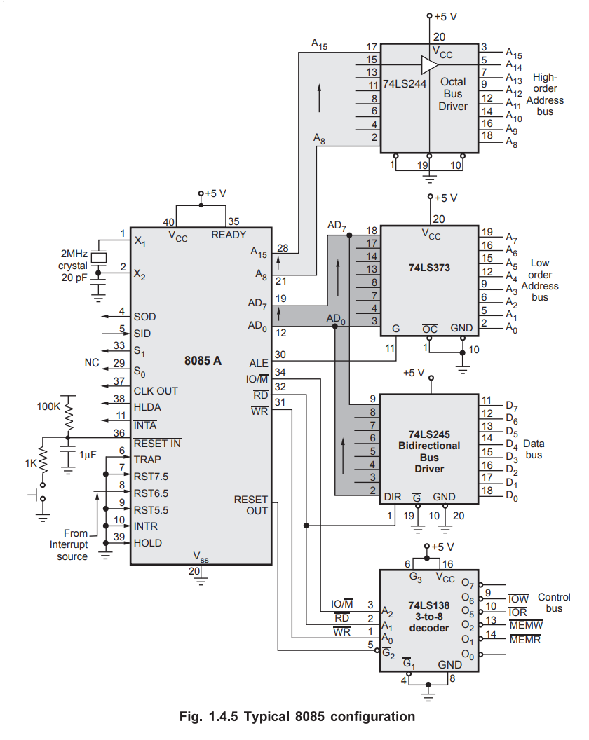
It
also shows clock and reset circuits. Interrupt lines which are not in use are
grounded. Similarly, since the DMA controller is not used, HOLD line is also
grounded. As we know READY signal is used to synchronize slow peripherals with
the microprocessor. When it is low, microprocessor enters in the wait state and
when it is high, it indicates that the memory or peripheral is ready to send or
receive data. Here, the READY signal is tied high to prevent the microprocessor
from entering the wait state. ALE signal is connected to the clock input of the
latch, to latch the low order address in Ti of the machine cycle. To control
the direction of the bi-directional buffer 74LS245, ![]() signal from 8085
is connected to DIR input of the bi-directional buffer. Thus, when
signal from 8085
is connected to DIR input of the bi-directional buffer. Thus, when ![]() signal is low, DIR is low and data flows from
memory or I/O device to the microprocessor, performing read operation. When
signal is low, DIR is low and data flows from
memory or I/O device to the microprocessor, performing read operation. When ![]() signal is high, DIR is high and data
flows from microprocessor to memory or I/O device performing write operation.
signal is high, DIR is high and data
flows from microprocessor to memory or I/O device performing write operation.
Review Questions
1. Draw the schematic
of latching low-order address bus in 8085 microprocessor.
AU : Dec.-11, Marks 2
2. Why AD0 – AD7 lines
are multiplexed?
3. Draw and explain
typical 8085 configuration.
4. Write a note on bus drivers.
Microprocessors and Microcontrollers: Unit I: (a) 8085 Processor : Tag: : Clock Circuit - Demultiplexing AD7 – AD0 - Reset Circuit - Typical Configuration - Bus Organization
Related Topics
Related Subjects
Microprocessor and Microcontroller
EE3404 MCU 4th Semester EEE Dept | 2021 Regulation | 4th Semester EEE Dept 2021 Regulation