Electron Devices and Circuits: Unit III: (a) BJT Amplifiers
CE, CB and CC Amplifiers
BJT Amplifiers
1. Common Emitter Amplifier Circuit 2. Common Collector Amplifier Circuit 3. Common Base Amplifier Circuit 4. Phase Relation between Input and Output
CE, CB and CC Amplifiers
1. Common Emitter Amplifier Circuit
•
Let us consider the common emitter amplifier circuit using self bias or voltage
divider bias as shown in the Fig. 6.1.1.

•
In the absence of input signal, only d.c. voltage are present in the circuit.
This is known as zero-signal or no-signal condition or quiescent condition for
the amplifier.
•
The d.c. collector-emitter voltage, VCE, the d.c. collector current Ic and d.c.
base current IB is the quiescent operating point for the amplifier.
•
On this d.c. quiescent operating point, we superimpose a.c. signal by
application of a.c. sinusoidal voltage at the input. Due to this base current
varies sinusoidally, as shown in Fig. 6.1.2.
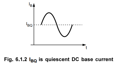
• As a result the collector current and the
output voltage, VCEQ will also vary sinusoidally about their quiescent values,
as shown in the Fig. 6.1.3 (a) and 6.1.3 (b).
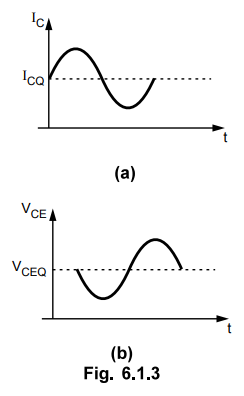
•
The collector current varies above and below its Q point value in-phase with
the base current, and the collector-to-emitter voltage varies above and below
its Q point value 180° out-of-phase with the base voltage.
•
Thus for common emitter amplifier, there is a phase shift of 180° between input
and output voltages.
•
When one cycle of input is completed, one cycle of output will also be
completed. This means the frequency of output sinusoidal is the same as the
frequency of input sinusoid.
•
Thus in the amplification process, frequency of the output signal does not
change, only the magnitude of the output is larger than that of the input.
•
The functions of components in the CE amplifier circuit are as follows :
1.
Biasing Circuit : The resistances Rr Rj and RE forms the
voltage divider biasing circuit for the CE amplifier. It sets the proper
operating point for the CE amplifier.
2.
Input Capacitor C1 : This capacitor couples
the signal to the base of the transistor. It blocks any d.c. component present
in the signal and passes only a.c. signal for amplification. Because of this
biasing conditions are maintained constant.
3.
Emitter Bypass Capacitor CE : An emitter bypass
capacitor C£ is connected in parallel with the emitter resistance, RE to
provide a low reactance path to the amplified a.c. signal. If it is not
inserted, the amplified a.c. signal passing through RE will cause a voltage
drop across it. This will reduce the output voltage, reducing the gain of the
amplifier.
4.
Output Coupling Capacitor C2 : The coupling
capacitor C2 couples the output of the amplifier to the load or to the next
stage of the amplifier. It blocks d.c. and passes only a.c. part of the
amplified signal.
2. Common Collector Amplifier Circuit
•
The Fig. 6.1.4 shows common collector circuit. The d.c. biasing is provided by
R1, R2 and RE . The load resistance is capacitor coupled to the emitter terminal
of the transistor.
•
When a signal is applied via to the base of the transistor, VB is increased and
decreased as the signal goes positive and negative, respectively.
•
Looking at Fig. 6.1.4 we can write that VE = VB – VBE.
Considering VBE fairly constant, we say that variation in the VB
appears at emitter and emitter voltage VE will vary same as base
voltage VB
•
Since the emitter is output terminal, it can be noted that the output voltage
from a common collector circuit is the same as its input voltage.
•
In other words, we can say that in common collector circuit emitter terminal
follows the signal voltage applied to the base. Hence the common collector
circuit is also known as an emitter follower.
3. Common Base Amplifier Circuit
•
Fig. 6.1.5 shows common base circuit. The signal source is coupled to the
emitter of the transistor via Ci- The load resistance RL is coupled to the
collector of the transistor via C2.
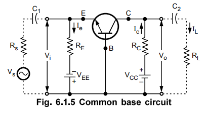
•
The positive going pulse of input source increases the emitter voltage. As base
voltage is constant, the forward bias of emitter base junction reduces. This reduces
Ib, reducing IC and hence the drop across
•
Since V = VCC- ICRC, the reduction in IC results in an increase in V. Therefore,
we can say that positive going input produces positive going output and
similarly negative going input produces negative going output and there is no
phase shift between input and output in a common base amplifier.
4. Phase Relation between Input and Output

1. Draw a typical common emitter amplifier and explain the
function of each component in it.
2. What is the need of coupling capacitors in amplifier design ?
3. Explain the working of a common emitter amplifier.
4. State the phase relationships between input/output currents
and between input/output voltages of various transistor configurations.
AU : Dec.-18, Marks 2
Electron Devices and Circuits: Unit III: (a) BJT Amplifiers : Tag: : BJT Amplifiers - CE, CB and CC Amplifiers
Related Topics
Related Subjects

Electron Devices and Circuits
EC3301 3rd Semester EEE Dept | 2021 Regulation | 3rd Semester EEE Dept 2021 Regulation