Linear Integrated Circuits: Unit III: Applications of Op-amp
Clamper Circuits using Op-amp
Working Principle, Pulse, Circuit Diagram, Applications | Operational amplifier
The circuits which are used to add a d.c. level as per the requirement, to the a.c. output are called as clamper circuits. Sometimes such circuits are also called as d.c. restorer circuits.
Clamper Circuits
Sometimes
it is necessary to add a d.c. level to the a.c. output signal. The circuits
which are used to add a d.c. level as per the requirement, to the a.c. output
are called as clamper circuits. Sometimes such circuits are also called as d.c.
restorer circuits. If the clamped d.c. level is positive, the circuits are
called as positive clamper circuits and if clamped d.c. level is negative, the
circuits are called as negative clamper circuits.
1. Positive Clamper Circuit
The
Fig. 3.22.1 shows the positive clamper circuit out
using op-amp.
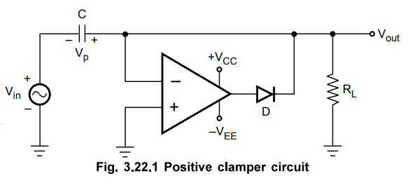
When
the input voltage Vil is first time negative, due to inverting mode of op-amp,
the op-amp output is positive. This turns on Fig.
3.22.1 Positive clamper circuit the diode making it forward biased. Thus the
capacitor charges to the peak value of the negative cycle of input with the
polarities as shown in the Fig. 3.22.1.
Just
beyond the negative input peak, the diode becomes reverse biased and stops
conducting. It becomes open. Hence the output voltage is sum of the input
voltage and the capacitor voltage mathematically it is given by,
Vout
= Vin + VP
Thus
the d.c. level equal to Vp gets added in the a.c. output signal. The final
output waveform is sinusoidal but shifted positively through Vp.
Hence the circuit is called positive clamper and the waveform is called
positively clamped waveform. As during positive half cycle of the input, diode
does not conduct, the capacitor retains its voltage at Vp all the time after
the first negative peak of the input.
The
waveforms are shown in the Fig. 3.22.2.
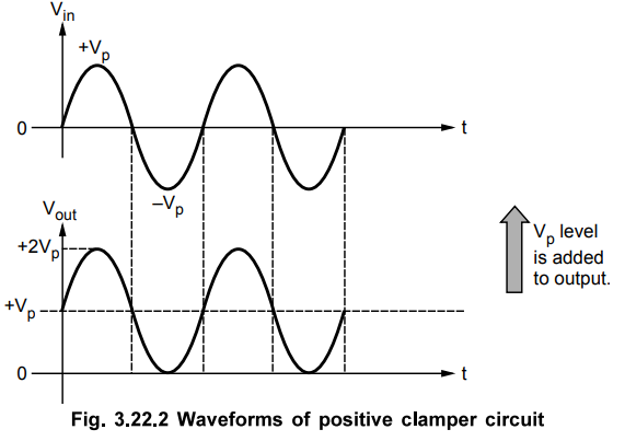
It
can be observed that output waveform swings from 0 to + 2 Vp i.e. peak to peak
voltage of output waveform is 2 Vp which remains same as the input voltage.
Thus the circuit shows that the total swing of the output voltage remains same
as the total swing of the input voltage in clamper circuit.
In
this circuit, the d.c. level added is equal to peak value of the input used.
Another circuit in which, variable positive d.c. level can be added is shown in
the Fig. 3.22.3.
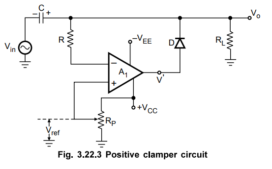
The
input voltage is applied to the inverting terminal of the op-amp A1 while
variable positive d.c. voltage is applied to the non-inverting input terminal
of the op-amp A1 The circuit can be analyzed using the Superposition
theorem considering only one input active at a time.
Let
Vref is acting alone and input Vin is zero. For positive Vref, the output
voltage V' is also positive. Due to this the diode D becomes forward biased.
Hence the circuit acts as a voltage follower. Hence the net output voltage Vo
is same as positive Vref.
Now
let input at inverting terminal be purely sinusoidal i.e. Vin = Vm
sin ωt. For negative half cycle of input, the V'o will be positive
and diode D will conduct. The capacitor C charges through diode D to the
negative peak voltage Vm. However during the positive half cycle of the input,
diode D does not conduct and capacitor C retains its previous voltage of Vin
This
voltage Vm is in series with the a.c. input voltage, the output
voltage becomes Vin + Vm.
Hence
the net output voltage due to the effect of both the inputs becomes Vin
+Vm + Vref
The
resistance R is used to protect the op-amp against excessive discharge currents
from the capacitor C, especially when the d.c. supply voltages are switched
off.
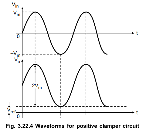
The
waveforms are shown in the Fig. 3.22.4.
As
the circuit clamps the peaks of the input waveforms hence the circuit is also
called as a peak clamper circuit.
2. Negative Clamper Circuit
The
Fig. 3.22.5 shows the negative clamper circuit obtained by reversing the diode
connections in positive clamper circuit.
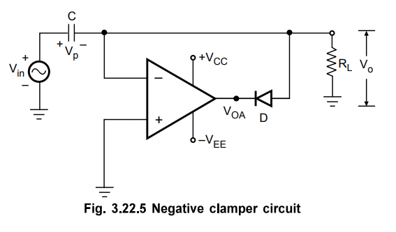
When
is first positive going, due to inverting mode of op-amp, the voltage VOA goes
negative. Thus diode D becomes forward biased and capacitor charges to peak
value with polarities as shown.
Just
beyond the positive peak, the diode becomes reverse biased and becomes open.
Hence the output voltage Vo is sum of the input and capacitor
voltages.
V
= Vin - Vp
Hence
a negative d.c. level of -Vp gets added to the output hence circuit
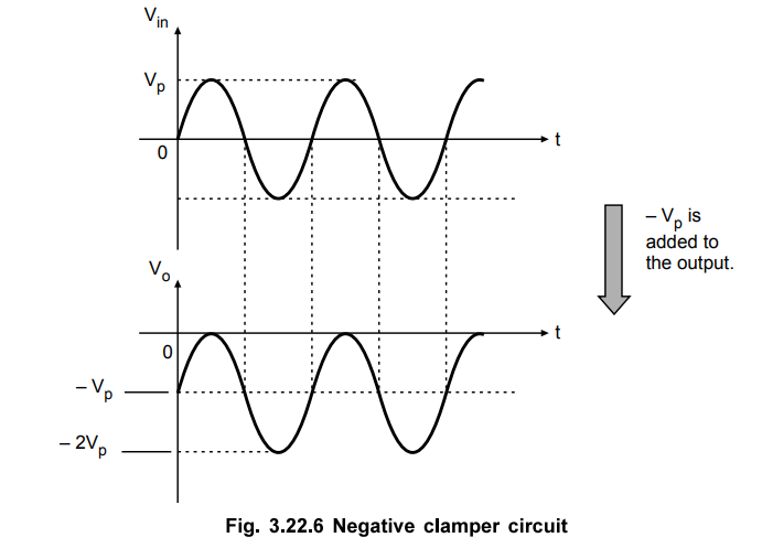
is called negative clamper circuit. The waveforms are shown in the Fig. 3.22.6.
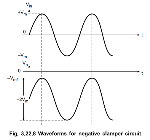
Another
circuit in which variable negative d.c. level can be added is shown in the Fig.
3.22.7. In such a circuit - Vref is generated using the negative
supply - VEE of the op-amp and the diode connections are reversed.

Due
to opposite connection of diode D, the capacitor charges in reverse direction
and hence negative clamper is obtained. The waveforms are shown in the Fig.
3.22.8.
3. Clamper Applications
The
clamper circuits are often used in the television receivers as d.c. restorer.
The video signal in television is processed through capacitively coupled
amplifiers hence the signal losts its d.c. component which effectively loses
black and white reference levels and the blanking level. Hence it is necessary
to restore these levels back before applying signal to the picture tube. This
is done by a clamper circuit acting as a d.c. restorer. This is shown in the Fig.
3.22.9.

Review Questions
1. Explain with neat
circuit diagram and the waveforms, the working of a negative clamper circuit.
2. Explain with neat
circuit diagram and the waveforms, the working of a positive clamper circuit.
3. Explain the
operation of op-amp as a clamper.
Dec.-09, 11, May-14, 17, Marks 8
Linear Integrated Circuits: Unit III: Applications of Op-amp : Tag: : Working Principle, Pulse, Circuit Diagram, Applications | Operational amplifier - Clamper Circuits using Op-amp
Related Topics
Related Subjects

Linear Integrated Circuits
EE3402 Lic Operational Amplifiers 4th Semester EEE Dept | 2021 Regulation | 4th Semester EEE Dept 2021 Regulation