Linear Integrated Circuits: Unit III: Applications of Op-amp
Clipper Circuits using Op-amp
Working Principle, Pulse, Circuit Diagram | Operational amplifier
The circuits which are used to clip off the unwanted portions of the input voltage above or below certain levels, so as to produce limited required output are called limiting circuits.
Clipper Circuits
The
circuits which are used to clip off the unwanted portions of the input voltage
above or below certain levels, so as to produce limited required output are
called limiting circuits. As some part of input gets clipped off to produce
output, these circuits are commonly called clipping circuits. These circuits
are classified as,
1.
Positive clipper circuit and 2. Negative clipper circuit.
The
positive clipper circuits remove some positive part from the input to produce
the output. The negative clipper circuits remove some negative part from the
input to produce the output.
1. Positive Clipper Circuit
A
positive clipper circuit using op-amp is shown in the Fig. 3.21.1.
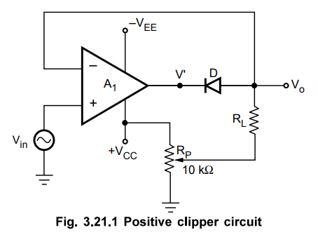
The
clipping level is determined by the reference voltage Vref. This
reference voltage is obtained from the positive supply voltage + VCC
or negative supply voltage -VEE. In the circuit shown the Vref
is determined by pot Rp, say 2 V.
In
the positive half cycle of the input, the diode D conducts till Vin =
Vref. When Vin is lee than Vref, the diode D
becomes forward biased and op-amp acts as a voltage follower. Hence the output
voltage Vo is same as Vin.
But
for Vin greater than Vref, the diode D becomes reverse
biased as V' is + Vsat and becomes open. This opens the feed back
loop and due to this, output voltage Vo remains at Vref
and entire waveform above Vref gets clipped off.
Thus
the diode is ON when Vin < Vref and OFF for Vin
> Vref. The output follows input when diode is on when it is
alternates between closed loop and open loop operation and hence op-amp used
must be high speed and compensated for unity gain. The high speed op-amp like
HA 2500, LM 310 and pA 318 can be used for such applications. The
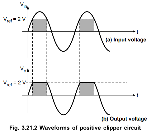
input and output waveforms are shown in the Fig. 3.21.2.
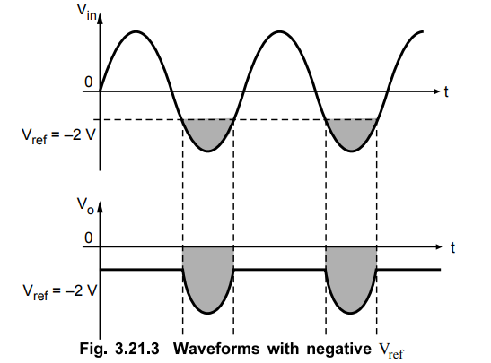
In
the same circuit if the pot Rp is used with - VEE to generate
negative Vref, instead of VCC then the entire waveforms
above - Vref gets clipped off. Let Vref = - 2 Vin
the same circuit, the output follows input only when Vin < Vref
i.e. Vin <-2V. The waveforms with Vref = -2 V are
shown in the Fig. 3.21.3.
2. Negative Clipper Circuit
The
negative clipper circuit can be obtained by reversing the connections of diode
D and using pot RP to generate negative reference voltage Vref.
This circuit is shown in the Fig. 3.21.4.
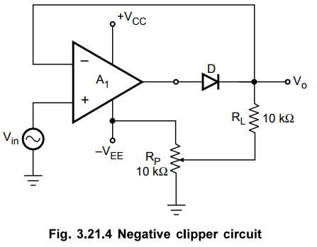
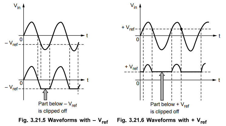
When Vin > - Vref, then the diode D conducts and the output voltage follows the input voltage. But when Vin < Vref' D is off and the voltage below - Vref gets clipped off. The circuit hence is called as negative clipper circuit. The waveforms are shown in the Fig. 3.21.4.
If
for the same circuit, reference voltage is generated using + VCC
i-e. + Vref then diode D is ON for Vin > Vref
and Vo = while diode D is OFF for < Vref and Vo
= Vref. The corresponding waveforms are shown in the Fig. 3.21.6.
Review Questions
1. Explain a positive clipper circuit using an op-amp and a
diode with neat diagrams.
April-10, May-17, Marks 8
2. Explain a negative clipper circuit using an op-amp and a
diode with neat diagrams.
3. Design a circuit of a clipper which will clip the input
signal below a reference voltage.
Dec.-15, Marks 8
Linear Integrated Circuits: Unit III: Applications of Op-amp : Tag: : Working Principle, Pulse, Circuit Diagram | Operational amplifier - Clipper Circuits using Op-amp
Related Topics
Related Subjects

Linear Integrated Circuits
EE3402 Lic Operational Amplifiers 4th Semester EEE Dept | 2021 Regulation | 4th Semester EEE Dept 2021 Regulation