Electron Devices and Circuits: Unit II: (b) Junction Field Effect Transistor (JEET)
Common Source Amplifier with self Bias (Unbypassed R3)
Junction Field Effect Transistor (JEET)
• Fig. 3.9.12 shows common source amplifier with self biasing having unbypassed Rs.
5. Common Source Amplifier with self Bias (Unbypassed R3)
• Fig. 3.9.12 shows common source amplifier with self biasing having unbypassed Rs.
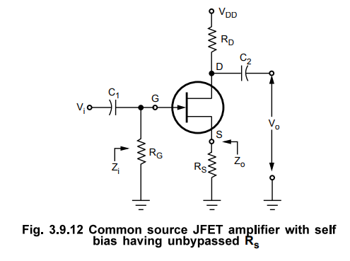
• Now Rs will be the part of low frequency equivalent model as shown in the Fig. 3.9.13.
Input impedance Zi :
• Looking into Fig. 3.9.13 we can say that,
Zi = R G ... (3.9.16)

• We observe that with unbypassed Rs the output impedance of circuit is increased, compare to when it is bypassed.
• We know that,
Zo = Zo '||RD
• Zo = [rd + Rs (p + 1)] II RD - (3.9.24)
or Zo = [rd + Rs (gm id+1)] IIRD ...(3.9.25)
Voltage Gain Av :
• It is given by,
Av = V0 / Vi
We know that,
Vo = - Id RD

Key Point: With unbypassed R5 voltage gain reduces.
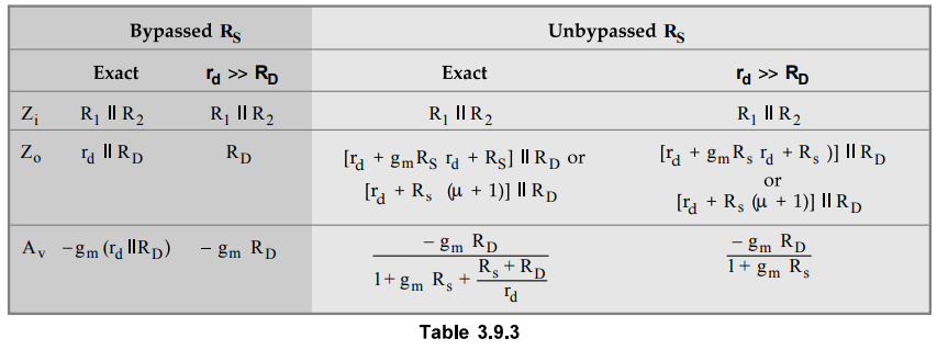
• Table 3.9.2 summarizes performance of common source amplifier with self bias.

Ex. 3.9.3 For common source amplifier as shown in Fig. 3.9.15 operating point is defined by VGS(-> = - 2.5 V, Vp = - 6 V and Id Ω = 2.5 mA with ldSS = 8 mA. Calculate gm , rd, Zl7 Zo and voltage gain Av.
Sol. :

6. Common Source Amplifier with Voltage Divider Bias (Bypassed Rs)
• Fig. 3.9.16 shows common source amplifier with voltage divider biasing.

• The coupling capacitor C and C2 which are used to isolate the d.c. biasing from the applied a.c. signal act as short circuits for the low frequency analysis. Bypass capacitor Cs also acts as short circuit for the low frequency analysis.
• Fig. 3.9.17 shows the low frequency equivalent model for the common source amplifier circuit with voltage divider bias. It is drawn by replacing :
• All capacitors and d.c. supply VDD with short circuits and,
• JFET with its low frequency equivalent circuit

• Since the resulting low frequency equivalent circuit is the same as a.c. equivalent circuit in Fig. 3.9.16, the equation for Zi , Zo and Av will be the same.
• It is important to note that, here,

• The negative sign in equation (3.9.41) again indicates there is a phase shift of 180° between input and output voltages.
7. Common Source Amplifier with Voltage Divider Bias (Unbypassed Rs)
• Fig. 3.9.18 shows common source amplifier with voltage divider bias having unbypassed Rs.

• Now Rs will be the part of a.c. equivalent model as shown in the Fig. 3.9.19
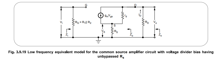
• Since the resulting a.c. equivalent circuit is the same as a.c. equivalent circuit in Fig. 3.9.14, the equation for Z;, Zo and Av will be the same.
• It is important to note that, here,

Ex. 3.9.4 For the amplifier shown in Fig. 3.9.20, calculate :
i) Av = Vo / Vi ii) Zi iii) Zo iv) Zo. Assume for FET gm = 2 mAIV, rd = 10 k Ω.

Sol. : The equivalent circuit for given circuit can be drawn as follows,


Table 3.9.3 summarizes the performance of common source amplifier with voltage divider bias.
Ex. 3.9.5 Draw the small signal equivalent circuit for FET of Fig. 3.9.22 and hence find and V02 /Vi in terms of circuit constants.

Sol. :

8. Common Drain Amplifier
• In common drain amplifier circuit input is applied between gate and source and output is taken between source and drain.
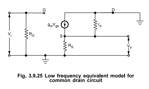
• Fig. 3.9.24 shows common drain configuration.

• It shows that the output is taken from source and when the d.c. supply is replaced by its short circuit equivalent the drain is grounded and thus common between input and output.
• In the common drain circuit the source voltage Vs is given as,
Vs = VG + VGS
• When a signal is applied to the JFET gate via Clz VG varies with the signal. As VGS is fairly constant and Vs = VG +VGS, Vs varies with V;. For example, if V; increases by 0.25 V, Vs also approximately increases by 0.25 V. Because the output voltage at the source (Vs) follows changes in the signal voltage applied to the gate, this circuit is also called as source follower.
• Fig. 3.9.25 shows the low frequency equivalent model for the common drain amplifier circuit shown in Fig. 3.9.24.
• This low frequency equivalent circuit can be simplified as shown in the Fig. 3.9.25
Input Impedance Zi :
Looking at Fig. 3.9.26, Z; can written as,
Zi = RG ... (3.9.49)

Output Impedance Zo : The output impedance is obtained by setting V; = 0 V. When Vi = 0, gate terminal is grounded. The resulted equivalent circuit is as shown in the Fig. 3.9.27
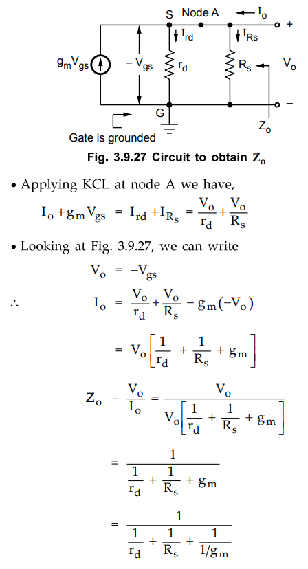
• The above equation represents the parallel combination of three resistors.

• Substituting values of Vo and V; from equations (3.9.54) and (3.9.55) respectively in above equation (3.9.57) we get,

Key Point :
1. We observe that the common drain circuit does not provide voltage gain.
2. The positive sign in equation (3.9.57) also indicates that there is no phase shift between input and output voltages.
• Table 3.9.4 summarizes the performance of common drain amplifier.

Ex. 3.9.6 For common drain amplifier as shown in Fig 3.9.28, gm = 2.5 mS, rd = 25 kΩ. Calculate , Zi, Zo and Av

Sol. :
Zi : We have,
Zi = RG = 1 MΩ
Zo : We have,

9. Common Gate Amplifier
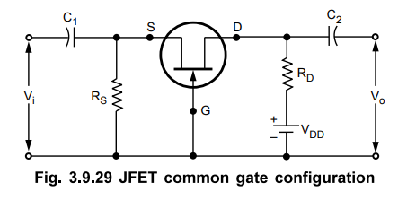
• In common gate amplifier circuit input is applied between source and gate and output is taken between drain and gate. Fig. 3.9.29 shows common gate configuration.
• In common gate configuration, gate voltage is at constant potential. Thus increase in input voltage Vj in positive direction increases the negative gate-source bias voltage. Due to this drain current reduces, reducing the drop IDRD- Since VD = VDD - IDRE>/ the reduction in ID results in an increase in output voltage (VD). Similarly when input voltage reduces, opposite action takes place which reduces the output voltage. Thus we can say that there is no phase shift between input and output in a common gate amplifier.
• Fig. 3.9.30 shows a.c. equivalent model for common gate amplifier circuit shown in Fig. 3.9.29.
Input impedance : It is given as,
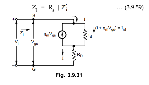
• Let us see the circuit in Fig. 3.9.31 for determining Zi. Zi is given by,
Zi = Vi / I
Looking at Fig. 3.9.31 we can say that, current through id
Key Point : Input resistance of CG amplifier is very less as compared to CS and CD amplifiers.
Output impedance Zo :
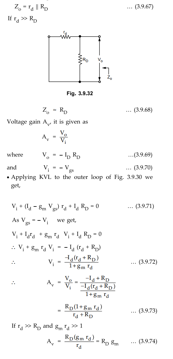
• It is the output impedance of the circuit when input is short circuited. Fig. 3.9.32 shows the a.c. equivalent model with input short circuited.
• As input is short circuited, Rg is also short circuited and Vgs becomes = 0 and hence V„„ = 0. Look at the gs gs
Fig. 3.9.32, ZQ can be given as,
Key Point : From equation (3.9.74) we observe that there is no phase shift between input and output in common gate amplifier.
• Table 3.9.5 summarizes the performance of common gate amplifier.

Ex. 3.9.7 For common gate amplifier as shown in the Fig. 3.9.33, gm = 2.8 mS, rd = 50 kΩ. Calculate Zr Zo and Av.

Review Questions
1. Explain how FET can be used as an amplifier.
2. Draw a small signal low frequency model for an FET and explain.
3. Write the equation from which the small signal low frequency equivalent circuit of JFET is formed.
4. Derive the expression for the voltage gain of i) Common source amplifier
ii) Common drain amplifier configurations, under small signal low frequency conditions.
AU : Dec.-04, Marks 16
5. Derive the expression for the voltage gain of : common drain amplifier configurations, under small signal low frequency conditions.
AU : May-05, Marks 8
6. Draw the characteristics of JFET and mark its regions of operation.
AU : Dec.-05, Marks 4
7. For a CS amplifier, draw the small signal equivalent circuit and determine expression for gain, input impedanace and output impedance.
AU ; May-14, Marks 8
Electron Devices and Circuits: Unit II: (b) Junction Field Effect Transistor (JEET) : Tag: : Junction Field Effect Transistor (JEET) - Common Source Amplifier with self Bias (Unbypassed R3)
Related Topics
Related Subjects

Electron Devices and Circuits
EC3301 3rd Semester EEE Dept | 2021 Regulation | 3rd Semester EEE Dept 2021 Regulation