Electron Devices and Circuits: Unit I: PN Junction Devices
Complete V-l Characteristics of a Diode
Effect of Temperature, Advantages, Disadvantages, Applications
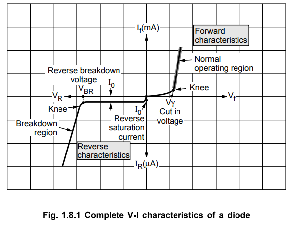
The complete V-I characteristics of a diode is the combination of its forward as well as reverse characteristics. This is shown in the Fig. 1.8.1.
Complete V-l Characteristics of a Diode
AU
: Dec.-05, 06, 09, 12, 13, 14, May-14,16
•
The complete V-I characteristics of a diode is the combination of its forward
as well as reverse characteristics. This is shown in the Fig. 1.8.1.
•
In forward characteristics, it is seen that initially forward current is small
as long as the bias voltage is less that the barrier potential. At a certain
voltage close to barrier potential, current increases rapidly. The voltage at
which diode current starts increasing rapidly is called as cut in voltage. It
is denoted by V. Below this voltage, current is less than 1 % of maximum rated
value of diode current. The cut-in voltage for germanium is about 0.2 V while
for silicon it is 0.6 V.
•
It is important to note that the breakdown voltage is much higher and
practically diodes are not operated in the breakdown condition. The voltage at
which breakdown occurs is called reverse breakdown voltage denoted as VBR.
Key
Point: Reverse current before the breakdown is very
very small and can be practically neglected.
1. V-l Characteristics of Typical Ge and SI Diodes
•
The combined for earlier, the barward and reverse characteristics is called V-I
characteristics of a diode. As mentionedrier potential for Germanium (Ge) diode
is about 0.3 V while for Silicon (Si) diode is as about 0.7 V. The potential at
which current starts increasing exponentially is also called Offset potential,
Threshold potential or Firing potential of a diode. The Fig. 1.8.2 shows the
V-I characteristics of typical Ge and Si diodes.
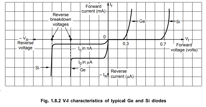
•
The reverse saturation current in a germanium diode is about 1000 times more
than the reverse saturation current in a silicon diode of a comparable rating.
The reverse saturation current IQ is of the order of nA for silicon diode while
it is of the order of uA for germanium diode. Reverse breakdown voltage for Si
diode is higher than that of the Ge diode of a comparable rating.
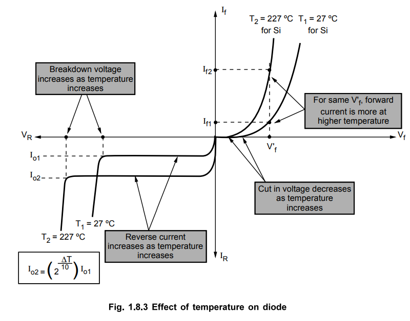
2. Effect of Temperature on p-n Junction Diode
•
The temperature has following effects on the diode parameters,
1.
The cut-in voltage decreases as the temperature increases. The diode conducts
at smaller voltages at large temperature.
2.
The reverse saturation current increases as temperature increases.
•
This increase in reverse current I0 is such that it doubles at every 10 °C rise
in temperature. Mathematically,
I02
= 2(ΔT/10) I01 … ΔT = (T2 – T1)
where
I02 = Reverse current at T2 °C and IQ1 = Reverse current
at T1 °C
3.
The voltage equivalent of temperature VT also increases as temperature
increases.
4.
The reverse breakdown voltage increases as temperature increases.
5.
The maximum safe value of power dissipation is mentioned in the datasheet of
the diode as (PD )max which is specified at normal room temperature of 25 °C.
At higher temperatures, as the device junction temperature is higher, it can
dissipate less power. Thus maximum power dissipation of the device decreases at
higher temperatures.
•
The effect of temperature on the diode characteristics is shown in the Fig.
1.8.3.
3. Advantages and Disadvantages of p-n Junction Diode
•
The various advantages of p-n junction diode are,
1.
It is very much compact and portable.
2.
If can be used as on-off switch.
3.
It has long life.
4.
It is operated with low voltage and has low power consumption.
5.
It is very cheap and readily available.
•
The various disadvantages of p-n junction diode are,
1.
It is temperature sensitive and its characteristics are affected due to changes
in temperature.
2.
While switching on-off, there is time delay hence not suitable for high speed
operations.
3.
Due to large reverse current, noise level is high.
4.
The power dissipation capability is low hence may get thermally destroyed.
5.
Requires finite voltage level to turn on which is undesirable in precise
applications.
4. Applications of p-n Junction Diode
•
The various application areas of p-n junction diode are,
1.
In rectifiers.
2.
In clipper and clamper circuits.
3.
In voltage multiplier circuits.
4.
In multivibrators.
5.
With op-amp, used in variety of applications such as precision rectifiers,
log-antilog amplifiers, oscillator amplitude stabilization circuits etc.
Review Questions
1. Draw and explain the V-I characteristics of a PN junction
diode.
AU : Dec.-05, 06, 09, 12, 14. May-14, 16, Harks 6
2. Explain the working of p-n junction diode and its V-I characteristics.
3. List advantages, disadvantages, applications of diode.
4. Discuss the effect of temperature on p-n junction diode.
Electron Devices and Circuits: Unit I: PN Junction Devices : Tag: : Effect of Temperature, Advantages, Disadvantages, Applications - Complete V-l Characteristics of a Diode
Related Topics
Related Subjects

Electron Devices and Circuits
EC3301 3rd Semester EEE Dept | 2021 Regulation | 3rd Semester EEE Dept 2021 Regulation