Linear Integrated Circuits: Unit II: Characteristics of Op-amp
D.C. Analysis of Differential Amplifier
Working Principle, Circuit Diagram, Solved Example Problems | Op-amp
The d.c. analysis means to obtain the operating point values i.e. ICQ and VCEQ for the transistors used.
D.C. Analysis of Differential Amplifier
May-06
The
d.c. analysis means to obtain the operating point values i.e. ICQ
and VCEQ for the transistors used. The supply voltages are d.c.
while the input signals are a.c., so d.c. equivalent circuit can be obtained
simply by reducing the input a.c. signals to zero. The d.c. equivalent circuit thus obtained is shown in the
Fig. 2.7.1. Assuming RS1 = RS2, the source resistance is
simply denoted by RS.

The
transistors Q1 and Q2 are matched transistors and hence
for such a matched pair we can assume :
i)
Both the transistors have the same characteristics.
ii)
RE1 = RE2 hence RE= RE1 || RE2
iii)
RC1 = RC2 hence denoted as RC.
iv)
| VCC | = | VEE | and both are measured with respect to
ground.
As
the two transistors are matched and circuit is symmetrical, it is enough to
find out operating point ICQ and VCEQ, for any one of the
two transistors. The same is applicable for the other transistor.
Applying
KVL to base-emitter loop of the transistor Q1,

From
the equation (2.7.6), we can observe that
i)
RE determines the emitter current of Q1 and Q2
for the known value of VEE
ii)
The emitter current through Q1 and Q2 is independent of
collector resistance RC.
Now
let us determine VCE. As IE is known and IE ≅ IC, we can
determine the collector voltage of Q1 as
VC
= VCC - ICRC ...(2.7.7)
Neglecting
the drop across RS we can say that the voltage at the emitter of Q1
is approximately equal to –VBE. Hence the collector to emitter
voltage is
VCE
- VC _ VE - (VCC _ ^R-C) _ ( _VBE)
VCE
- VCC + VBE_ICRC ...(2.7.8)
Hence
IE = IC = ICQ while VCE = VCEQ
for given values of VCC and VEE.
Key
Point In the equation (2.7.6), the sign of VEE
is already considered to be negative, while deriving it. Hence while using this
equation to solve the problem, only the magnitude of VEE should be
used and negative sign of VEE should not be used again.
Thus
for both the transistors, we can determine operating point values, using
equations (2.7.6) and (2.7.8). With the same biasing arrangement, the d.c.
analysis remains same for all the four possible configurations of differential
amplifier.

Key
Point The d.c. analysis and expressions for ICQ
and VCEQ remain same for all the differential amplifier circuit configurations.
Example
2.7.1 Calculate the operating point values for the circuit shown in the Fig.
2.7.2.
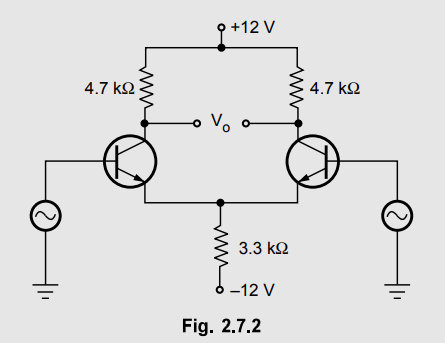
Solution
:
From the Fig. 2.7.2 we can write
RC
= 4.7 k Ω,
RE = 3.3 k Ω, VCC = 12V, VEE =
-12V
From
equation (2.7.6),
IE
= VEE – VBE / 2 RE
The
sign of VEE is already considered while deriving the euqtion hence VEE
must be replaced by 12 V. And assume VBE = 0.7 V.

Review Questions
1. Draw the circuit
diagram of emitter coupled differential amplifier and obtain its d.c. analysis
2. Calculate the operating point values for the transistors
shown in the Fig. 2.7.3.
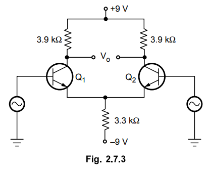
[ Ans.: 1.25 mA, 4.825 V ]
3. For a differential amplifier circuit operated from ± 5 V, assume VBE = 0.7 V and hfe
= 100. If Rc for each is 100 k Ω, calculate the value of RE so that the quiescent
collector emitter voltage for each transistor is 4 V.
[ Ans.: 125 k Ω ]
Linear Integrated Circuits: Unit II: Characteristics of Op-amp : Tag: : Working Principle, Circuit Diagram, Solved Example Problems | Op-amp - D.C. Analysis of Differential Amplifier
Related Topics
Related Subjects

Linear Integrated Circuits
EE3402 Lic Operational Amplifiers 4th Semester EEE Dept | 2021 Regulation | 4th Semester EEE Dept 2021 Regulation