Linear Integrated Circuits: Unit III: Applications of Op-amp
DAC (Digital to Analog Converter) using Op-amp
Performance Parameters, Working Principle, Circuit Diagram, Types, Solved Example Problems | Operational amplifier
A DAC (Digital to Analog Converter) accepts an n-bit input word b1, b2, b3, ... bn in binary and produce an analog signal proportional to it.
D/A Converters
May-03,
04, 05, 06, 07, 08, 09, 10, 11, 12, 15, 17,
Dec.-03,
04, 05, 06, 07, 08, 09, 10, 11, 12, 17
A
DAC (Digital to Analog Converter) accepts an n-bit input word b1, b2,
b3, ... bn in binary and produce an analog signal
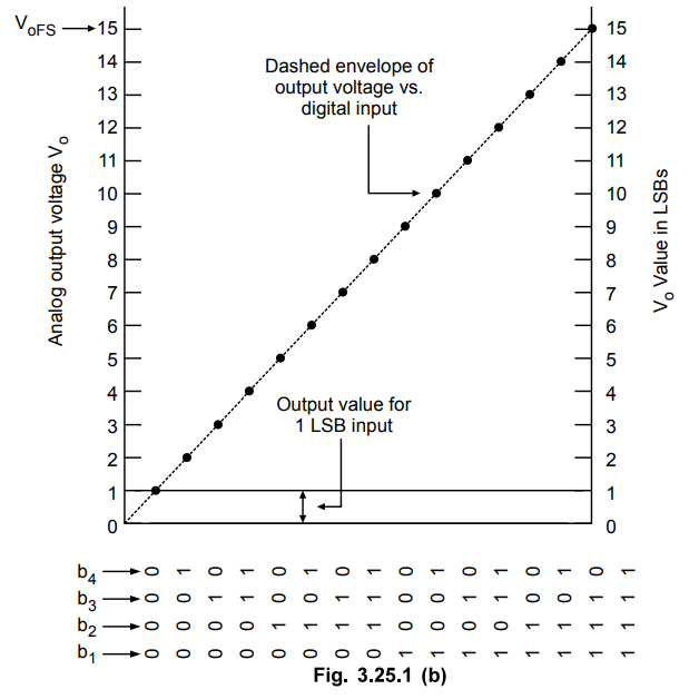
proportional to it. Fig. 3.25.1 shows circuit symbol and input-output characteristics
of a 4-bit DAC. There are four digital inputs, indicating 4-bit DAC. Each
digital input requires an electrical signal representing either a logic 1 or a logic
0. The bn is the least significant bit, LSB, whereas b 1 is the most
significant bit, MSB.
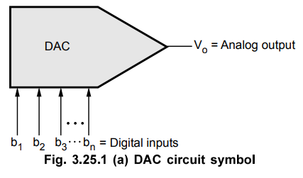
Fig.
3.25.1 (b) shows analog output voltage Vo is plotted against all 16 possible
digital input words.
1. Performance Parameters of DAC
The
various performance parameters of DAC are,
a.
Resolution
Resolution
is defined in two ways.
•
Resolution is the number of different analog output values that can be provided
by a DAC. For an n-bit DAC
Resolution
= 2n ... (3.25.1)
•
Resolution is also defined as the ratio of a change in output voltage resulting
from a change of 1 LSB at the digital inputs. For an n-bit DAC it can be given
as
Resolution
= VoFS / 2n – 1 ... (3.25.2)
where, VoFS = Full scale output voltage
From
equation (3.25.1), we can say that, the resolution can be determined by the
number of bits in the input binary word. For an 8-bit DAC resolution can be
given as
Resolution
= 2n = 28
=
256
If
the full scale output voltage is 10.2 V then by second definition the
resolution for an 8-bit DAC can be given as
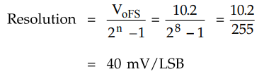
Therefore,
we can say that an input change of 1 LSB causes the output to change by 40 mV.
From
the resolution, we can obtain the input-output equation for a DAC.
Thus Vo = Resolution × D
where D = Decimal
value of the digital input
and Vo = Output voltage
The
resolution takes care of changes in the input.
b.
Accuracy
It
is a comparison of actual output voltage with expected output. It is expressed
in percentage. Ideally, the accuracy of DAC should be, at worst, ± 1/2 its LSB. If the full scale output voltage
is 10.2 V then for an 8-bit DAC accuracy can be given as
Accuracy
= VoFS / (2n – 1)2 ….
(3.25.3)
=
10.2 / 255 × 2 = 20mV
c.
Monotonicity
A
converter is said to have good monotonicity if it does not miss any step
backward when stepped through its entire range by a counter.
d.
Conversion Time
It
is a time required for conversion of analog signal into its digital equivalent.
It is also called setting time. It depends on the response time of the switches
and the output of the amplifier.
e.
Settling Time
This
is the time required for the output of the DAC to settle to within ±1/2 LSB of
the final value for a given digital input i.e. zero to full scale.
f.
Stability
The
performance of converter changes with temperature, age and power supply
variations. So all the relevant parameters such as offset, gain, linearity
error and monotonicity must be specified over the full temperature and power
supply ranges. These parameters represent the stability of the converter.
Example
3.25.1 An 8-bit DAC has an output voltage range of 0-2.55
V. Define its resolution in two ways.
Solution
:
For the given DAC,
n
= Number of bits = 8
i)
Resolution = 2n = 28 = 256
i.e.
the output voltage can have 256 different values including zero.
ii)
VoFS = Full scale output voltage
=
2.55 V
Resolution
= VoFS / 2n -1 = 2.55 / 28 - 1
10mV
/ 1 LSB
Thus
an input change of 1 LSB causes the output to change by 10 mV.
Example
3.25.2 The digital input for a 4-bit DAC is 0110.
Calculate its final output voltage.
Solution
:
For given DAC,
n
= 4
VoFS
= 15 V
Resolution
= VoFS / 2n -1 = 15 / 24 – 1 = 1V/LSB
Vo
= Resolution × D
Now
D = Decimal of (0110)2 = 6
Vo
= 1 V/LSB × 6 = 6 V
Example
3.25.3 An 8-bit DAC has resolution of 20 mV/LSB. Find VoFS
and Vo if the input is (10000000)2.
Solution
:
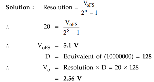
Example
3.25.4 Find out stepsize and analog output for
4-bit R-2R ladder DAC when input is 1000 and 1111. Assume Vref = +5
V.
Solution : For given DAC, n = 4, VoFS = +5 V
Resolution
= VoFS / 2n-1 = 5 / 24-1
= 1/ 3 V / LSB
Vo
= Resolution × D
For
= Decimal of (1000)2 = 8
Vo
= 1/ 3 × 8 = 2.6667 V
For D = Decimal of (1111)2 =15
Vo
= 1 / 3 ×15 = 5V.
Example
3.25.5 A 12-bit DAC has a step size of 8 mV. Determine
the full scale output voltage and percentage resolution. Also find the output
voltage for the input of 010101101101?
Solution
:
For 12-bit DAC, step size is 8 mV.
VoFS
= 8mV × 212 -1 = 32.76 V 8mV
%
Resolution = 8mV / 32.76V × 100 = 0.02442 %
The
output voltage for the input 010101101101 is = 8 mV × (1389)10 =
11.112 V
Example
3.25.6 Determine the output voltage produced by a 4-bit DAC
whose output voltage range is 0 to 10 V when the input binary number is 0110.
Dec.-03,
Marks 6
Solution
:
Given VoFS = 10 V
Resolution
= 10 / 24 – 1 = 0.6667 V
The
output voltage at 0110 = 0.6667 × 6 = 4 V
Example
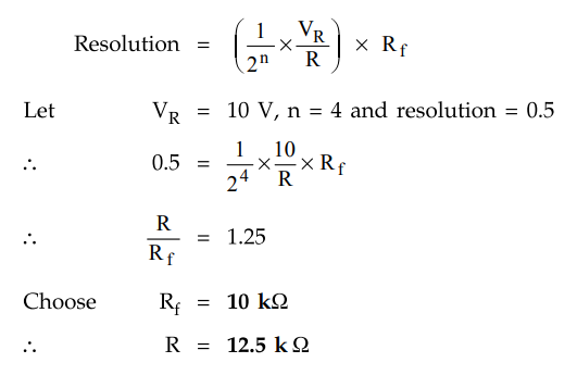
3.25.7 Suggest the values of resistors and reference
voltage if resolution required is 0.5 V for 4-bit R/2R ladder type DAC.
Solution
:
2. Types of D/A Converter
There
are mainly two techniques used for analog to digital conversion
•
Binary weighted resistor D/A converter
•
R/2R ladder D/A converter
In
these techniques, the shunt resistors are used to generate n binary weighted
currents. These currents are added according to switch positions controlled by
the digital input and then converted into voltage to give analog voltage equivalent
to the digital input. Therefore, such digital to analog converters are called
current driven DACs.
a.
Binary Weighted Resistor D/A Converter
The
binary weighted resistor DAC uses an op-amp to sum n binary weighted currents
derived from a reference voltage VR via current scaling resistors 2R, 4R, 8R,
..., 2n R, as shown in the Fig. 3.25.2

As
shown in the Fig. 3.25.2, switch positions are controlled by the digital
inputs. When digital input is logic 1, it connects the corresponding resistance
to the reference voltage VR; otherwise it leaves resistor open. Therefore,
For
ON-switch, I = VR / R and
For
OFF-switch, I = 0
Here,
operational amplifier is used as a summing amplifier. Due to high input
impedance of op-amp, summing current will flow through Rf. Hence the total
current through Rf can be given as
IT
= I0 +I1 + I2 + … + In
The
output voltage is the voltage across Rf and it is given as
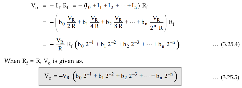
The
equation (3.25.4) indicates that the analog output voltage is proportional to
the input digital word.
The
simplicity of the binary weighted DAC is offset by drawbacks associated with
it.
Drawbacks
:
1.
Wide range of resistor values are required. For 8-bit DAC, the resistors
required are 21 R, 22 R, 23 R,... and 28 R.
Therefore, the largest resistor is 128 times the smallest one.
2.
This wide range of resistor values has restrictions on both, higher and lower
ends. It is impracticable to fabricate large values of resistor in IC, and
voltage drop across such a large resistor due to the bias current also affects
the accuracy. For smaller values of resistors, the loading effect may occur.
3.
The finite resistance of the switches disturbs the binary-weighted relationship
among the various currents, particularly in the most significant bit positions,
where the current setting resistances are smaller.
All
these drawbacks, especially the requirement of wide range of resistors
restricts the use of binary weighted resistor DACs below 8-bits.
b.
Inverted R-2R Ladder I Current Mode R-2R Ladder D/A Converter
R/2R
ladder D/A converter uses only two resistor values. This avoids resistance
spread drawback of binary weighted D/A converter. Fig. 3.25.3 shows R/2R ladder
DAC. Like binary weighted resistor DAC, it also uses shunt resistors to
generate n binary weighted currents; however it uses voltage scaling and
identical resistors instead of resistor scaling and common voltage reference
used in binary weighted resistor DAC. Voltage scaling requires an additional
set of voltage dropping series resistances between adjacent nodes, as shown in
the Fig. 3.25.3.
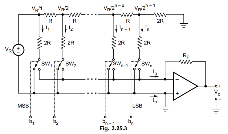
Here,
each bit of the binary word connects the corresponding switch either to ground
or to the inverting input terminal of the op-amp which is at the virtual
ground. Since both the positions of switches are at ground potential, the
current flowing through resistances is constant and it is independent of switch
position. These currents can be given as,
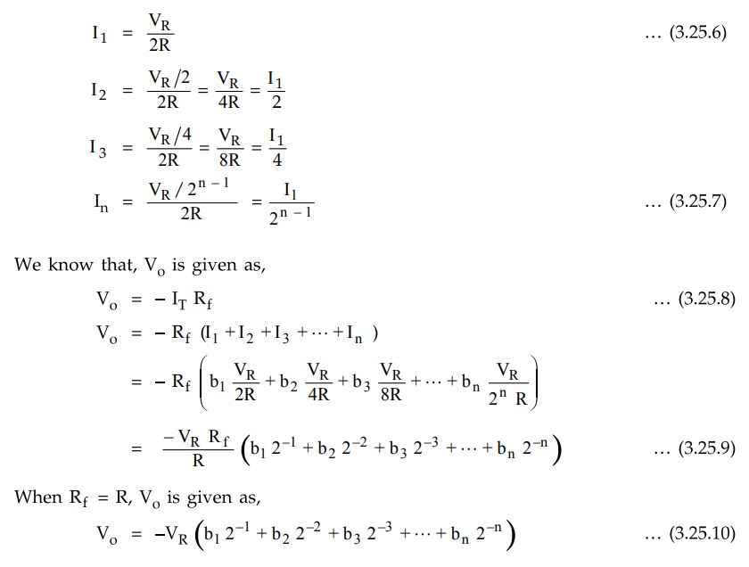
Let
us consider 4-bit binary DAC with binary input 1001 and Rf = R, as shown in the
Fig. 3.25.4.
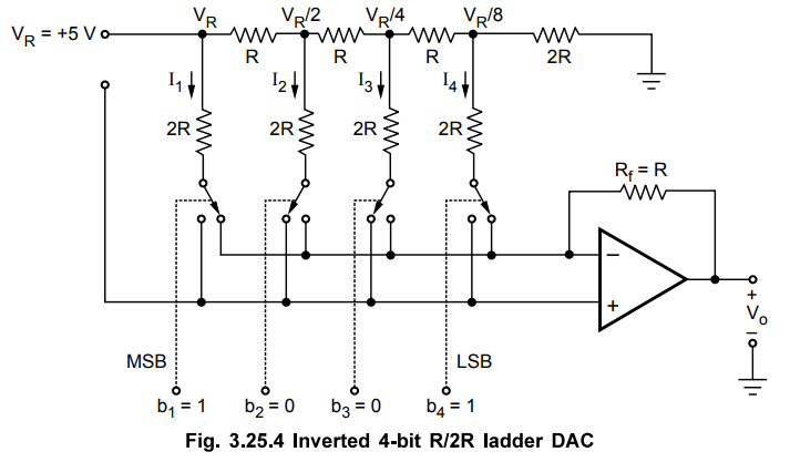
Here,
output voltage is given as
The
inverting R/2R ladder DAC works on the principle of summing currents and it is
also said to operate in the current steering mode. An important advantage of
the current mode is that all ladder node voltages remain constant with changing
input codes, thus avoiding any shutdown effects by stray capacitances.
c.
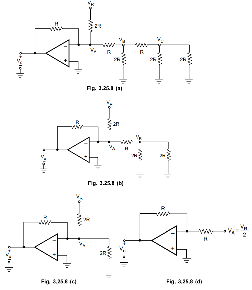
R-2R Ladder I Voltage Mode R-2R Ladder D/A Converter
In
this type, reference voltage is applied to one of the switch positions, and
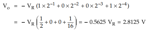
other switch position is connected to ground, as shown in the Fig. 3.25.5.
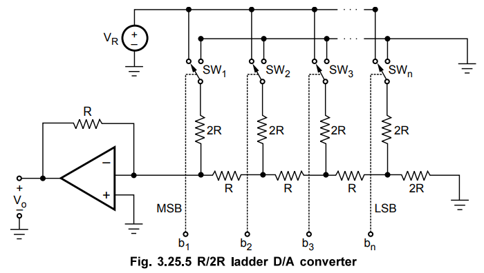
Let
us consider 3-bit R/2R ladder DAC with binary input 001, as shown in the Fig.
3.25.6.
Reducing
above network to the left by Thevenin's theorem we get,
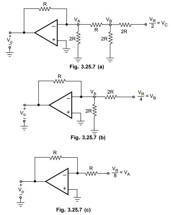
Therefore,
the output voltage is VR/8 which is equivalent to binary input 001. For binary
input 100 the network can be reduced as follows :
Therefore,
the output voltage is VR/2, which is equivalent to binary input 100.
In general, the voltage is given by

The
expression for Vo can be obtained as,
Let
Iout - Output current
Rf
= Feedback resistance of op-amp
Vo
= - Iout Rf
Now
Iout = Current resolution × D
Vo
= (Current resolution × D) Rf
Vo
= (Current resolution × Rf) × D
….. (3.25.11)
The
coefficient of D is the voltage resolution and can be called simple resolution.
Vo
= - Resolution ×D (Binary data) ...
(3.25.12)
In
terms of actual circuit elements, output can be written as,
Vo
= - (VR / R × 1 / 2n
Rf ….. (3.25.13)
The
resolution of R/2R ladder type DAC with current output is,
Resolution
= 1 / 2n × VR / R
… (3.25.15)
while
the resolution for R/2R ladder type DAC with voltage output is,
Resolution
= (1 / 2n × VR / R) × Rf … (3.15.15)
3. Sources of Errors in DAC
There
are mainly three errors in DACs : Linearity, Offset and gain errors.
a.
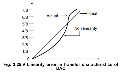
Linearity Error
The
error is defined as the amount by which the actual output differs from the
ideal straight-line output.
Fig.
3.25.9 shows the linearity error in the transfer characteristics of DAC. It is
mainly due to the errors in the current source resistor values
b.
Offset Error
The
offset error is defined as the nonzero level of the output voltage when all
inputs are zero.
It
adds a constant value to all output values, as shown in Fig. 3.25.10.

It
is due to the presence of offset voltage in op-amp and leakage currents in the
current switches.
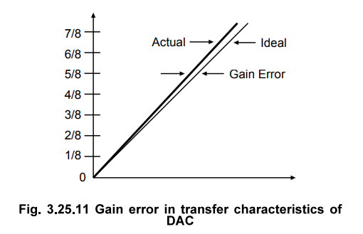
c.
Gain Error
The
gain error is defined as the difference between the calculated gain of the
current to voltage converter and the actual gain achieved. It is due to the
errors in the feedback resistor on the current to voltage converter op-amp.
Fig.
3.25.11 shows the gain error in transfer characteristics of DAC.
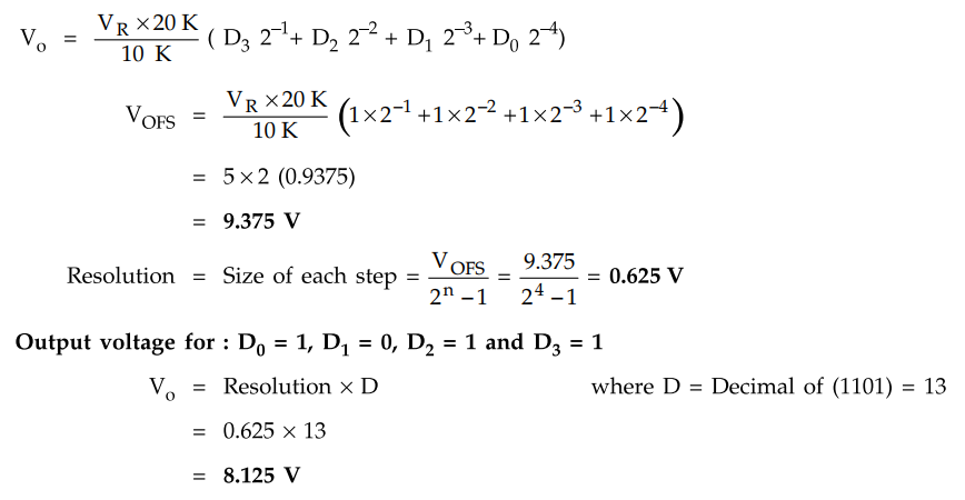
Example
3.25.8 Design a 4 bit R-2R ladder network, determine the
size of each step if R = 10 kΩ, Rf = 20 kΩ and VCC = ± 15
V. Calculate the output voltage for Do = 1, D1 = 0, D2
= 1 and D3 = 1 if bit '1' applied as 5 V and bit 'O' applied
as 0 V.
May-13,
Marks 8
Solution
:
Fig. 3.25.12 shows 4-bit R-2R ladder.
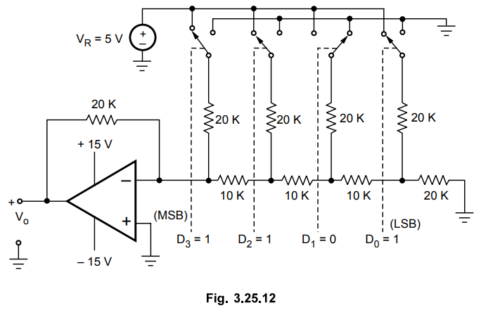
The
output voltage for DAC shown in Fig. 3.25.12 is given by
Review Questions
1. Explain the
weighted resistor DAC with neat sketch.
May-06, Dec.-11, 17,
Marks 8
2. Explain in detail
about R-2R ladder DAC and inverted R-2R ladder DAC alongwith relevant circuit
diagrams and waveforms.
Dec.-03, 07,09,
May-04, 06, 11, Marks 16
3. Explain the
important DAC specifications.
May-12, Dec.-12, Marks
4
4. With neat circuit diagram
explain the operation of R-2R D/A converter
May-15, 17, Dec.-17, Marks 8
Linear Integrated Circuits: Unit III: Applications of Op-amp : Tag: : Performance Parameters, Working Principle, Circuit Diagram, Types, Solved Example Problems | Operational amplifier - DAC (Digital to Analog Converter) using Op-amp
Related Topics
Related Subjects

Linear Integrated Circuits
EE3402 Lic Operational Amplifiers 4th Semester EEE Dept | 2021 Regulation | 4th Semester EEE Dept 2021 Regulation