Electron Devices and Circuits: Unit I: PN Junction Devices
Derivation of V-l Characteristics of P-N Junction Diode
Let us study the derivation of the mathematical expression for the current through a diode, which gives its V-I characteristics.
Derivation of V-l Characteristics of P-N Junction Diode
Let
us study the derivation of the mathematical expression for the current through
a diode, which gives its V-I characteristics.
Let Pp = Hole concentration in
p-type at the edge of depletion region
Nn
= Electron concentration in n-type at the edge of depletion region
Pn
= Hole concentration in n-type at the edge of depletion region
np
= Electron concentration in p-type at the edge of depletion region
Key
Point : Note that in the symbol, basic letter indicates
type of charge carrier concentration hole (p) or electron (n). The base
indicates type of material in which it exists.
•
Under unbiased condition, when holes move from p-side to n-side due to
diffusion, their concentration behaves exponentially. This is mathematically
expressed as,
Pp
= Pn eVj/VT ...(1.10.1)
where Vj = Barrier potential or
junction potential
•
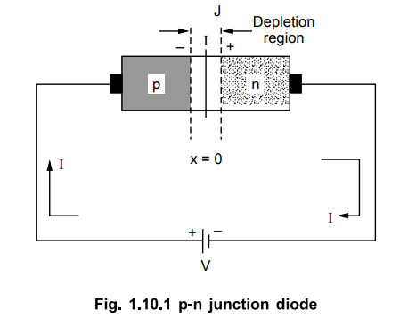
Now consider forward biased diode as shown in the Fig. 1.10.1. The junction is
at x = 0.
•
Though the proportion of holes and electrons in constituting a current through
the p-region is changing, the hole concentration throughout the entire p-region
is constant and denoted as,
Pp0
= Hole concentration in p-region
•
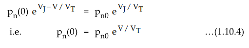
As holes cross the junction, this concentration becomes pn(0) which
is concentration of holes on n-side just near the junction. This further
behaves exponentially as given in the equation (1.10.1). From equation (1.10.1)
we can write,
Pp0
= Pn (0) e(Vj/V) / VT … (1.10.2)
Key
Point : The term Vj becomes Vj - V as the forward biased
voltage V opposes the barrier potential. So net voltage across the junction
becomes Vj – V.
•
The equation (1.10.2) can be written for open circuited unbiased p-n junction
diode by putting V = 0 as,
Pp0
= Pn (0) eVj/VT … (1.10.3)
•
where pn0 is the concentration of holes on n-side just near the
junction when diode is open circuited i.e. at thermal equilibrium and hence
different than Pn(0).
•
As the concentration of holes in entire p-region is constant, equating
equations (1.10.2) and (1.10.3) we get,
•
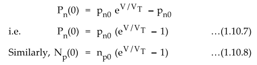
This equation represents boundary condition and called law of junction. This
indicates that the hole concentration pn(0) at the junction under forward
biased condition is greater than its thermal equilibrium value pn0.
For large forward biasing pn(0) becomes much larger compared to pn0.
Key
Point : The discussion is equally applicable
for the electron concentration on the p-side.
Thus,
np(0) = npo eV/VT ...(1.10.5)
•
Now the difference between two concentrations at the junction under unbiased
and biased condition is called injected or excess concentration denoted as Pn(0)'
Pn(0)
= Pn (0) – Pn0 …. (1.10.6)
•
Using equation (1.10.4) in equation (1.10.6),
•
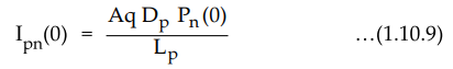
The hole current crossing the junction from p-side to n-side is given by,
•
While an electron current crossing the junction from n-side to p-side is given
by,
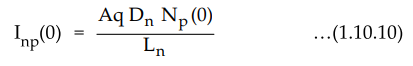
where A = Area of cross-section of
junction,
Dp
= Diffusion constant for holes P
Dn
= Diffusion constant for electrons,
Lp
= Diffusion length for holes
Ln
= Diffusion length for electrons
•
Using equations (1.10.7) and (1.10.8) in equations (1.10.9) and (1.10.10), the
total current I at the junction is given by,
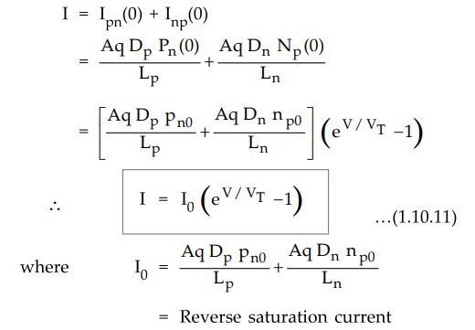
•
The equation (1.10.11) is the required expression for diode current.
Key
Point : In the derivation, the generation and
recombination in the depletion region is neglected. To consider its effect,
which is dominant in Si diodes, the factor q is introduced in the equation.
I
= I0 (e V/ηVT – 1) … (1.10.12)
•
The value of q = 1 for Ge diodes and η = 2 for Si diodes.
Review Question
1. Derive the p-n diode current equation.
AU : May-11, Marks 8
Electron Devices and Circuits: Unit I: PN Junction Devices : Tag: : - Derivation of V-l Characteristics of P-N Junction Diode
Related Topics
Related Subjects

Electron Devices and Circuits
EC3301 3rd Semester EEE Dept | 2021 Regulation | 3rd Semester EEE Dept 2021 Regulation