Electron Devices and Circuits: Unit II: (a) Bipolar Junction Transistors (BJT)
Different Biasing Circuits
Bipolar Junction Transistors (BJT)
• The different biasing circuits are : • Fixed bias circuit • Collector to base bias circuit • Voltage divider / self bias circuit • Emitter stabilized bias circuit • Miscellaneous bias circuit
Different Biasing Circuits
AU
: Dec.-02,04,05,06,08,10,11,13,15,17,18,May-04,05,06,11,12,17
•
The different biasing circuits are :
•
Fixed bias circuit
•
Collector to base bias circuit
•
Voltage divider / self bias circuit
•
Emitter stabilized bias circuit
•
Miscellaneous bias circuit
•
In section 2.5.2 we have already studied fixed bias circuit. Here, we will see
the advantages and disadvantages of fixed bias circuit and study the other
biasing circuits.
1. Fixed Bias using a pnp Transistor
The
Fig. 2.8.1 shows the fixed bias circuit for pnp transistor.
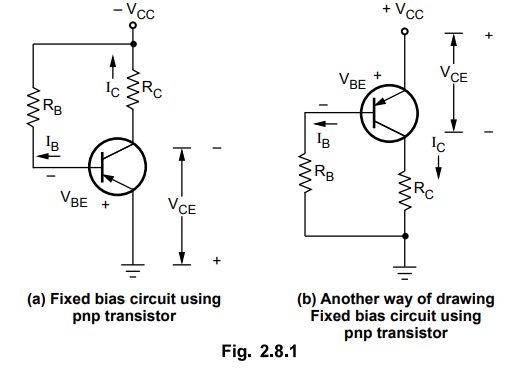
•
Here, the voltage polarities and current directions are reversed than that of
npn transistor fixed bias circuit.
•
However, the equations applied for the analysis of npn transistor fixed bias
circuit can be applied for the analysis of pnp transistor fixed bias circuit.
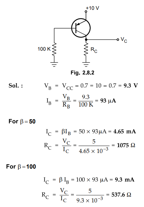
Ex.
2.8.1 The pnp transistor in the circuit of Fig. 2.8.2 has Beta = 50. Find the
valves of Rc to obtain Vc = 5 V. What happens if the transistor is replaced
with another Beta = 100 ?
2. Advantages and Disadvantages of Fixed Bias Circuit
Advantages
of Fixed Bias Circuit
1.
This is a simple circuit which uses very few components.
2.
The operating point can be fixed anywhere in the active region of the
characteristics by simply changing the value of Thus, it provides maximum
flexibility in the design.
Disadvantages
of Fixed Bias Circuit
1.
This circuit does not provide any check on the collector current which
increases with the rise in temperature, i.e. thermal stability is not provided
by this circuit. So the operating point is not maintained.
IC
= β IB + ICEO
2.
Since IC = β IB and IB is already fixed; IC depends on P
which changes unit to unit and shifts the operating point.
3.
Thus stabilization of operating point is very poor in the fixed bias circuit.
Important
Concept
If
the transistor is replaced by another transistor, eventhough the type is same
their characteristic may differ slightly. In fixed bias circuit, the change in
the characteristic of transistor changes the operating point. For example, if
there is a change in value of P there is change in IC = P IB as IB is constant
in fixed biased circuit. The change in IC changes the operating point and hence
we can say that a fixed bias circuit is unsatisfactory if the transistor is
replaced by another of the same type.
3. Collector to Base Bias Circuit
•
The Fig. 2.8.3 shows the dc bias with voltage feedback. It is also called the
collector to base bias circuit.

•
In this the biasing resistor is connected between the collector and the base of
the transistor to provide a feedback path. Thus IB flows through RB
and (IC + IB) flows through the RC.
a.
Circuit Analysis
Base
Circuit
•
Let us consider the base circuit of Fig. 2.8.3. Applying KVL to the base
circuit we get,
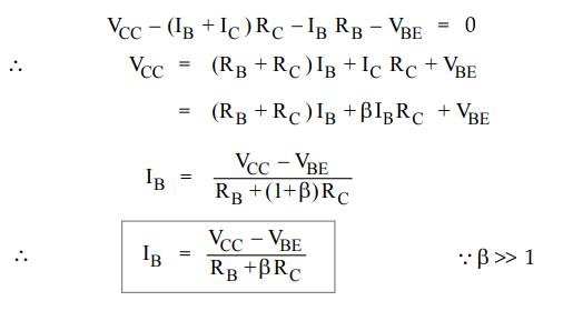
•
Note that the only difference between the equation for IB and that obtained for
the fixed bias configuration is the term PRC. Thus, we can say that the
feedback path results in a reflection of the resistance RC to the input
circuit.
Collector
Circuit
•
Applying KVL to the collector circuit we get,
VCC
- (I C + I B ) RC - VCE = 0
VCE
= VCC - (IC + IB ) RC
•
If there is a change in β due to piece to piece variation between transistors or
if there is a change in β and ICO due to the change in temperature,
then collector current IC tends to increase, since
IC
= β IB +ICEO
•
As a result, voltage drop across RC increases. Since supply voltage
VCC is constant, due to increase in IC RC, VCE
decreases. Due to reduction in VE IB reduces.
•
As IC depends on IB decrease in IB reduces the
original increase in IC. The result is that the circuit tends to
maintain a stable value of collector current, keeping the Q point fixed.
•
In this circuit, RB appears directly across input (base) and output
(collector). A part of the output is fed back to the input, and increase in
collector current decreases the base current. Thus negative feedback exists in
the circuit, so this circuit is also called voltage feedback bias circuit.
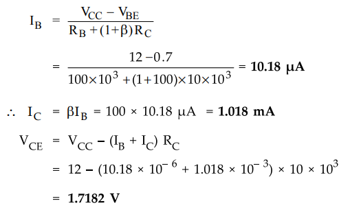
Ex.
2.8.2 Calculate the Q point values (IC
and VCE) for the circuit in Fig. 2.8.4.

Sol :
Ex.
2.8.3 Calculate the minimum and maximum values of Ic and VCE for the collector
to base bias when hFE (min) = 50 and hFE (max) = 60. For circuit, Vcc = 12 V,
Rc = 2 K and RB = 150 K. Assume silicon transistor.

Important
Concept
Comparing
the results of examples 2.1.2 and 2.4.3 we can say that collector to base bias
circuit provides more bias stabilization than base bias.
Ex.
2.8.4 Design a collector to base bias circuit to have operating point of (10 V,
4 mA). The circuit is supplied with 20 V and uses a silicon transistor of hfe
= 250.
Sol.
:

b.
Stability Factors for Collector to Base Bias Circuit
Stability
factor S
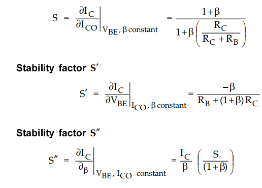
Ex.
2.8.5 Derive the expression for the stability factor S for collector to base
bias circuit.
Sol.
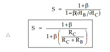
: Step 1 : Obtain the value of ∂IB / ∂IC

For
collector to base bias we have
Differentiating
w.r.t. IC and considering VBE to be independent of IC we
get,
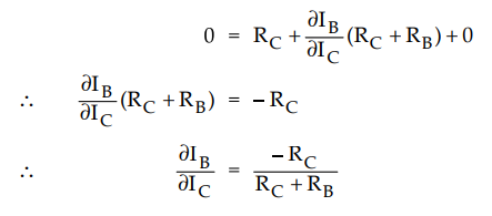
Step
2 : Substitute the value of ∂IB / ∂IC in expression of S
c.
Collector to Base Bias using pnp Transistor
•
The Fig. 2.8.6 shows the collector to base bias for pnp transistor.

•
Here, the voltage polarities and current directions are reversed than that of
npn transistor collector to base bias circuit.
•
However, the equations applied for the analysis of npn transistor collector to
base bias circuit can be applied for the analysis of pnp transistor collector
to base bias circuit.
4. Voltage Divider Bias, Self Bias or Emitter Bias
•
A circuit which is used to establish a stable operating point is the
self-biasing circuit shown in Fig. 2.8.7. This circuit is also known as voltage
divider bias circuit.

•
In this circuit, the biasing is provided by three resistors : R1 R2
and RE.
•
The resistors R1 and R2 act as a potential divider giving
a fixed voltage to point B which is base.
•
If collector current increases due to change in β temperature or change in ft
the emitter current IE also increases and the voltage drop across RE increases,
reducing the voltage difference between base and emitter (VBE).
•
Due to reduction in VBE, base current IB and hence
collector current Ic also reduces. Therefore, we can say that negative feedback
exists in the voltage divider bias circuit.
•
This reduction in collector current IC compensates for the original change in IC.
a.
Circuit Analysis
Base
circuit
•
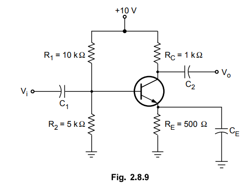
Fig. 2.8.8 shows Thevenin's equivalent circuit of voltage divider bias. Here, R
and R2 are replaced by RB and VT, where RB is the parallel combination of R and
R and VT is the Thevenin's voltage. RB can be calculated as
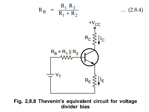
Applying
KVL to the base circuit of Fig. 2.8.8 we get,
Collector
Circuit
Applying
KVL to collector circuit we have,
VCE
= VCC - ICRC
- IERE
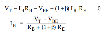
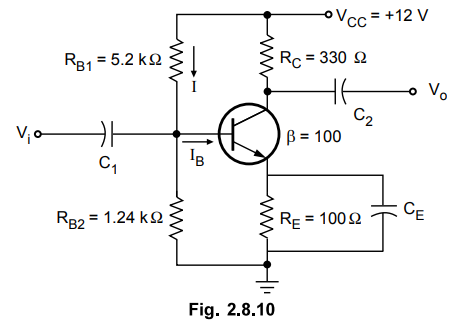
Ex.
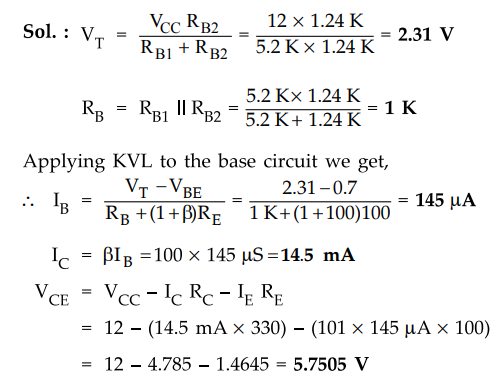
2.8.6 For the circuit shown in Fig. 2.8.9, ft = 200 for the silicon transistor.
Calculate VCE and IC.
Sol :
Applying
KVL to the base circuit we get,
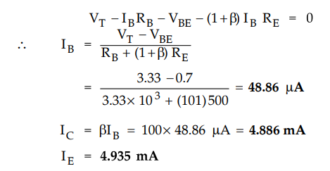
Applying
KVL to collector circuit we have,
VCE
= VCC - ICRC - ERE
=
10 - 4.886 × 1 - 4.935 × 0.5 = 2.6465 V
Ex.
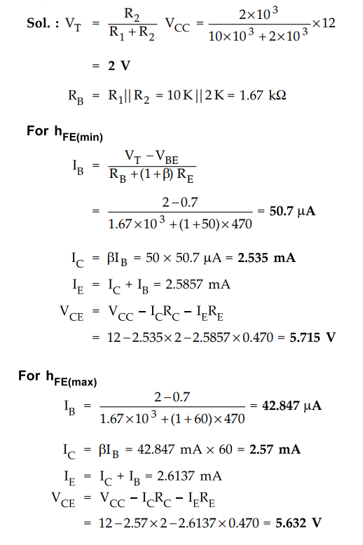
2.8.7 Calculate the minimum and maximum values of Ic and VCE for the
voltage divider bias circuit when hfe (min) = 50 and hFE(max) = 60. For circuit
VCC = 12 V, R1 = 10 K, R2 = 2 K, RE = 470 Q and RC = 2 K. Assume silicon
transistor.
Sol
:
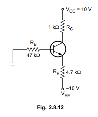
Ex.
2.8.8 Draw the d.c. load line for the following transistor configuration.
Obtain the quiescent point.
Sol.
:
The
d.c. load line for the above circuit can be drawn as shown in the Fig. 2.8.11.
Ex.
2.8.9 Find the Q point of the transistor shown below. Also draw the d.c. load
line. Given : β = 100 and VBE = 0-7 V.
AU
: Dec.-18, Marks 15
Sol :

b. Stability Factors for Self Bias S
Stability factor S

Important
Concept
It
is clear from equation (2.8.5) that minimizing S also minimizes S". This
means that the ratio RB/RE must be small to have better stability factor
S".
Ex.
2.8.10 Derive the expression for the stability factor S of the voltage divider
bias circuit. Comment on result.
Sol.
: Step 1 : Obtain the value of ∂I B/ ∂I C
•
Fig. 2.8.14 shows the Thevenin's equivalent circuit for voltage divider bias.
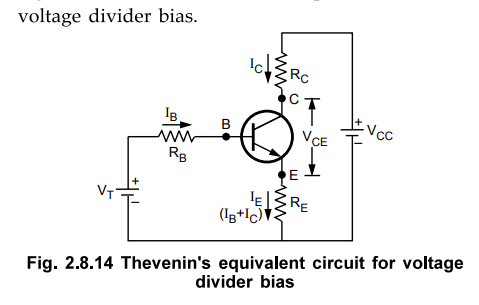
• Applying KVL to the base circuit we get,
VT
= IB RB + VBB + (IB +IC)
RE
•
Differentiating w.r.t. IC and considering VBE to be independent of
IC we get,

Step
2 : Substitute the value of ∂I B/ ∂I C in expression of S

Important
Concept
1.
The ratio RB/RE controls value of stability factor S. If
RB/RE << 1 then
S
= (1 + β) . 1 / (1 + β) = 1
Practically
RB/RE ≠ 0. But to have better stability factor S we have
to keep ratio RB/RE as small as possible.
2.
To keep RB/RE small, it is necessary to keep RB small.
This means that Rj II R 2 must be small. Due to small value of RE and R2,
potential divider circuit will draw more current from VCC reducing
the life of the battery. So while designing if we make R2 much smaller than RE
then parallel combination results small RB without drawing more current through
VCC. Another important aspect is that reducing RB will reduce input
impedance of the circuit, since RB comes in parallel with the input. This
reduction of input impedance in amplifier circuits is not desirable and hence
RB cannot be made very small.
3.
Emitter resistance RE is the another parameter we can use to decrease ratio
RB/RE. By increasing RE we can make RB/RE small. But as we increase RE, drop
IEREwill also increase and since VCC is constant, drop across RC will reduce.
This shifts the operating point Q which is not desirable and hence there is
limit for increasing RE¬
Thus
while designing voltage divider bias circuit we have to keep in mind :
S
– Should be small
RE
– Should be reasonably small
RE
– Should not be very large
4.
If ratio RB/RE is fixed, S increases with β. Therefore
stability decreases with increasing β
5.
Stability factor S is essentially independent of P for small value of S.
Ex. 2.8.11 For a circuit shown in Fig. 2.8.15, Vcc = 20V, Rc = 2k Ω, β = 50, VBE = 0.2 V, Rt = 100 k Ω, R2 = 10 k Ω, RE = 100 Ω. Calculate IB, VCE, lc and stability factor S.
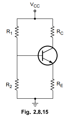
Sol.

Ex.
2.8.12 Design a voltage divider bias circuit for transistor to establish the
quiescent point at VCE = 12 V, Ic = 1.5 mA, stability factor S ≤ 3, β = 50, VBE = 0.7 V, Vcc = 22.5 V and RC = 5.6
k Ω.
AU
: May-17, Marks 15
Sol.
: Step 1 : Calculate RE
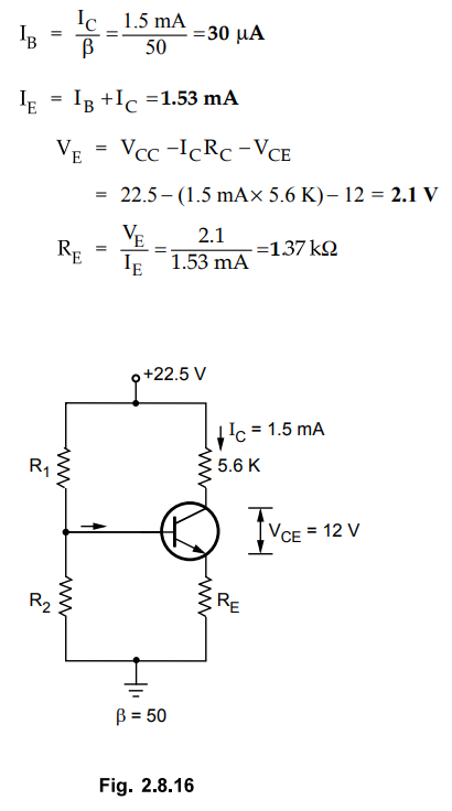
Step
2 : Calculate RB
We
know that, stability factor for self bias circuit is

Since
S should be ≤ 3, RB should be ≤ 2.91 k Ω
Let
us take RB = 3 K
Step
3 : Calculate R1 and R2

c.
Voltage Divider Bias using pnp Transistor
•
The Fig. 2.8.18 shows the voltage divider bias using pnp transistor.
•
Here, the positions of RE and RC are changed according to the terminals of
transistor. The voltage VB is measured across resistor Ri instead of resistor
R2-
•
Like other biasing circuits using pnp transistor, the current and voltage
polarities are reverse of those in npn transistor.
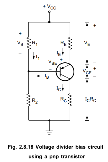
•
Apart from these changes, a pnp transistor voltage divider bias circuit is
analysed in exactly the same way as an npn transistor circuit.
5. Comparison of Biassing Circuits
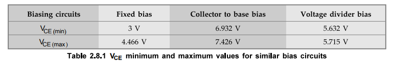
•
We have seen that the biasing circuit should provide the stability of Q point
against the change in device parameters. In examples 2.5.2, 2.8.3 and 2.8.7 we
have seen the Q point calculations for each biasing circuits against the change
in h FE (β).
•
The VCE values calculated for each circuit for hFE (min) and hFE (max) are listed Table 2-8-1 Each circuit uses 12 V supply and has 2 kQ
collector (load) resistance. On the basis of these similarities if we compare
VCE values of these circuits. We can observe following points.
• The collector to fixed bias provides more
stability than the fixed bias circuit.
• Voltage divider bias provides the
greatest stability against hFE variations.
•
Because of its excellent stability, voltage divider bias is the most commonly
used biasing circuit.
•
The Table 2.8.2 gives the comparison between the biasing circuits.

Review Questions
1. What are the types
of transistor biasing ? AU : ECE : Dec.-ll, Marks 2
2. Explain different
types of biasing circuits. AU : ECE : Dec.-06, Marks 16
3. Draw the self bias
circuit. AU : ECE : May-06, Dec.-08, Marks 2
4. Draw a self
(voltage divider) bias and derive all the stability factors S, S' and S".
AU : ECE : Dec.-lO,
13, Marks 16; May-08, 10
5. Derive the
expression of stability factor for collector feedback amplifier.
6. Draw the single
stage self-biased circuit using pnp transistor.
7. Draw the circuit
diagram of self-bias circuit using CE configuration and explain how it
stabilizes operating point.
8. What is the
advantage of using emitter resistance in the context of biasing ?
9. Describe the
stability in fixed bias and self bias and compare their performance.
10. Prove that self
bias is better bias compared to collector to base bias.
11. Prove that
collector to base bias is better than fixed bias.
12. Derive the
stability factor δIc / δhfz in a self bias circuit. What are the design considerations
to make the stability factor independent of hfz variation
AU : ECE : Dec.-05,
Marks 10
13. Draw a voltage
divider bias BJT network. Derive expressions for ICQ and VCEQ and describe the method
of drawing the d.c. load line on the output characteristics of transistor.
AU : ECE : May-12, Marks 16
14. Comment on fixed
biasing in BJT. Explain the procedure for locating suitable operating point on
the characteristic curves. AU : ECE : May-12, Marks 10
15. Explain the
emitter bias method used in transistor amplifier circuits.
AU : Dec.-17, Marks 5
Electron Devices and Circuits: Unit II: (a) Bipolar Junction Transistors (BJT) : Tag: : Bipolar Junction Transistors (BJT) - Different Biasing Circuits
Related Topics
Related Subjects

Electron Devices and Circuits
EC3301 3rd Semester EEE Dept | 2021 Regulation | 3rd Semester EEE Dept 2021 Regulation