Microprocessors and Microcontrollers: Unit V: (a) Microcontroller Applications
Display Interface
1. LED Interface 2. Multiplexed 7-Segment Display Interfacing 3. LCD Interfacing
Display Interface
1. LED Interface
•
Sourcing current : It refers to the maximum current that
the 8051 port pin can supply to drive an externally connected device. The
device can be an LED, a buzzer or TTL logic device. For TTL family of 8051
devices the sourcing current is approximately 60 µA.
•
Sinking current : If refers to the maximum current that
the 8051 port pin can absorb through a device which is connected to an external
supply. Pins of P1, P2 and P3 can sink a maximum current of 1.6 mA. Port 0 pins
can sink current upto 3.2 mA.
•
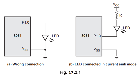
A typical LED consumes 10 to 15 mA. Thus we cannot drive LED directly in
current source mode as shown in the Fig. 17.2.1 (a). However, we can drive LED
directly in current sink mode, as shown in the Fig. 17.2.1 (b). Here, sinking
current of 8051 is not enough to drive LED, so the brightness of LED is poor.
•
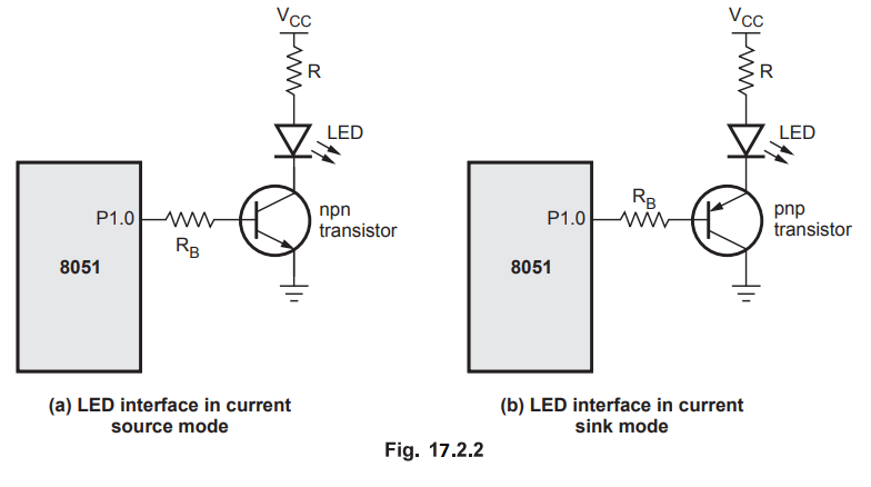
We can use driver transistor to solve the problem of current sinking and
sourcing. The Fig. 17.2.2 shows the LED interface using driver transistor.
•
In Fig. 17.2.2 (a), the source current of 8051 port pin is amplified by the npn
transistor to drive the LED. In Fig. 17.2.2 (b), the pnp transistor is used to
amplify the sinking current.
R
= VCC - VLED / ILED
RB
= Vout – VBE / (ILED / β)
where
VLED is the voltage across LED
ILED
is the current through LED
Vout
is the voltage at output pin
β
is the current gain (Beta) of the transistor
Example
17.2.1 Write an ALP to flash the LED connected to port
P2.0.
AU
: Dec.-13, Marks 2
Solution
:
Algorithm 1
Step
1: Make P2.0 High
Step
2: Wait for some time
Step
3: Make P2.0 LOW
Step
4: Wait for some time
Step
5: Repeat steps 1 through step 4
Algorithm
2
Step
1: Complement P2.0
Step
2: Wait for some time
Step
3: Repeat steps 1 and 2
Program
1:
ORG
0000H
BACK:
SETB P2.0 ; Make P2.0 high
ACALL
Delay ; Wait for some time
CLR
P2.0 ; Make P2.0 low
ACALL
Delay ; Wait for some time
SJMP
BACK ; repeat
Program
2:
ORG
0000H
BACK:
CPL P2.0 ; Complement P2.0
ACALL
Delay ; Wait for some time
SJMP
BACK
2. Multiplexed 7-Segment Display Interfacing
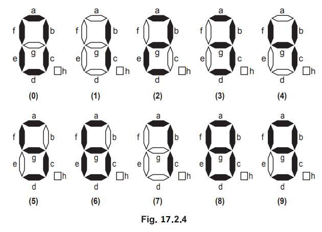
Seven-segment
display : Seven-segment displays are generally used as
numerical indicators and consists of a number of LEDs arranged in seven-segments
as shown in the Fig. 17.2.3.
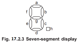
Any
number between 0 and 9 can be indicated by lighting the appropriate segments.
The
seven-segments are labelled a to g and dot is labelled as h. By forward biasing
different LED segments, we can display the digits 0 through 9. For instance, to
display 0, we need to light up a, b, c, d, e, and f. To light up 5, we need
segments a, f, g, c and d.
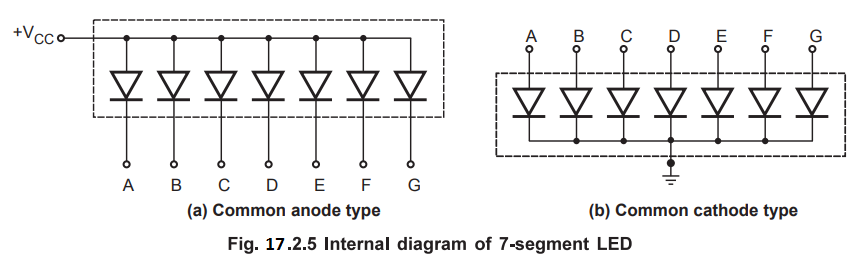
These
7-segment displays are of two types :
•
Common anode type
•
Common cathode type
In
common anode, all anodes of LEDs are connected together as shown in Fig. 17.2.5
(a) and in common cathode, all cathodes are connected together, as shown in
Fig. 17.2.5 (b).
Static
display
Fig.
17.2.6 shows a circuit to drive a single, seven-segment, common anode LED
display. For common anode, when anode is connected to positive supply, a low
voltage is applied to a cathode to turn it on. Here, BCD to seven-segment
decoder, IC 7447 is used to apply low voltages at cathodes according to BCD
input applied to IC 7447. To limit the current through LED segments resistors
are connected in series with the segments. This circuit connection is referred
to as a static display because current is being passed through the display at
all times.
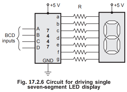
The
value of the resistor in series with the segment can be calculated as follows :
We
know, VCC - Drop across LED segment - IR = 0
Drop
across LED segment is nearly 1.5 V.
ஃ
IR
- VCC - 1.5 V = 5 - 1.5 V
=
3.5 V
Each
LED segment requires a current of between 5 and 30 mA to light. Let's assume
that current through LED segment is 15 mA.
ஃ R = 3.5 V /
15mA = 233 Ω
In
practice, the voltage drop across the LED and the output of IC 7447 are not
exactly predictable and the exact current through the LED is not critical as
long as we don't exceed its maximum current rating. Therefore, a standard value
220 Ω can be used.
The
static display circuits work well for driving just one or two LED digits.
However, these circuits are not suitable for driving more LED digits, say 8
digits. When there are more number of digits, the first problem is power
consumption. For worst case calculations, assume that all eight digits with all
segments are lit. Therefore, worst case current required is
1
= 8 (digits) × 7 (segment) × 15 mA (current per segment)
=
840 mA
A
second problem of the static approach is that each display digit requires a
separate BCD to 7-segment decoder.
Multiplexed
display
To
solve the problems of the static display approach, multiplexed display method
is used. Fig. 17.2.7 shows the 4 seven-segment displays connected using
multiplexed method. Here, common anode seven-segment LEDs are used.
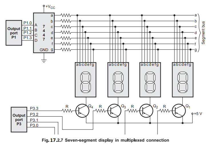
Anodes
are connected to +5 V through transistors. Cathodes of all seven-segments are
connected in parallel and then to the output of 7447 IC through resistors.
Looking at the Fig. 17.2.7 the question may occur in our mind that,"Aren't
all of the digits going to display the same number?" The answer is that
they would show the same number only if all the digits are turned on at the
same time. However, in multiplexed display the segment information is sent for
all digits on the common lines (output lines of IC 7447), but only one display
digit is turned on at a time. The PNP transistors connected in series with the
common anode of each digit act as an ON and OFF switch for that digit. Here's
how the multiplexing process works.
The
BCD code for digit 1 is first output from port 1, to the IC 7447. The IC 7447,
BCD to seven-segment decoder outputs the corresponding seven-segment code on
the segment bus lines. The transistor Q1 connected to digit 1 is
then turned on by outputting a low to that bit of port 3. All of the rest of
the bits of port 3 are made high to ensure no other digits are turned on. After
2 ms, digit 1 is turned OFF outputting all highs to port 3. The BCD code for
digit 2 is then output to the port 1, and bit pattern to turn on digit 2 is
output on port 3. After 2 ms, digit 2 is turned off and the process is repeated
for digit 3 and digit 4. After completion of turn for each digit, all the
digits are lit again in turn.
With
4 digits and 2 ms per digit we get back to digit 1 every 8 ms or about 125
times a second. This refresh rate is fast enough that, to our eye and due to
persistence of vision all digits will appear to be lit all the time.
In
multiplexed display, the segment current is kept in between 40 mA to 60 mA so
that they will appear as bright as they would if not multiplexed. Even with
this increased segment current, multiplexing gives a large saving in power and
hardware components.
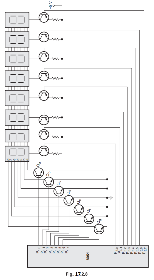
Example
17.2.2 Interface an 8-bit 7-segment LED display to 8051
through port 1 and port 3 and write an 8051 assembly language program to
display message on the display.
Solution
: Hardware
The
Fig. 17.2.8 shows the multiplexed 8-digit 7-segment LED display connected in
8051 system using port 1 and port 3. In this circuit port 1 and port 3 are used
as a latch, i.e. output port. Port 1 provides the segment data inputs to the
display and port 3 provides a means of selecting a display position at a time
for multiplexing the displays. Here, instead of BCD to seven-segment decoder
(IC 7447) transistors are used to drive the LED segments. Due to this we can
also display HEX characters on the display; however in this case we have to
send the proper 7-segment code of a particular digit that is to be displayed on
the port 1.
Subroutine to Display Message
MOV
R0, #8H ; Initialize counter
MOV
R1, #7FH ; load select pattern
MOV
DPTR, #6000H ; Starting address of message to be displayed
AGAIN
: MOV P3, R1 ; select digit
MOVX
A, @DPTR ; Get data
MOV
P1, A ; Send data
LCALL
DELAY ; Wait for some time
MOV
A, R1 ; [ Adjust
RR
A ; selection
MOV
R1, A ; pattern]
INC
DPTR ; Increment message pointer
DJNZ
R0, AGAIN ; Decrement R0 and check
RET
; if for zero; if not, goto AGAIN
Note
This subroutine must be called continuously to display the 7-segment coded message
stored in the memory from address 6000H.
3. LCD Interfacing
Now-a-days,
many LCD modules are available which have built-in drivers for LCD and
interfacing circuitry to interface them to microprocessor/microcontroller
systems. These LCD modules allow display of characters as well as numbers. They
are available in 16 × 2, 20 × 1, 20 × 2, 20 × 4 and 40 × 2 sizes. The main
advantage of using LCD is modules is that they require very less power. The
first figure represents number of character in each line and second figure
represents number of lines the display has. In this section, we see the
interfacing of 20 × 2 LCD display module to microprocessor/microcontroller
system through 8255. In this module the display is organized as two lines, each
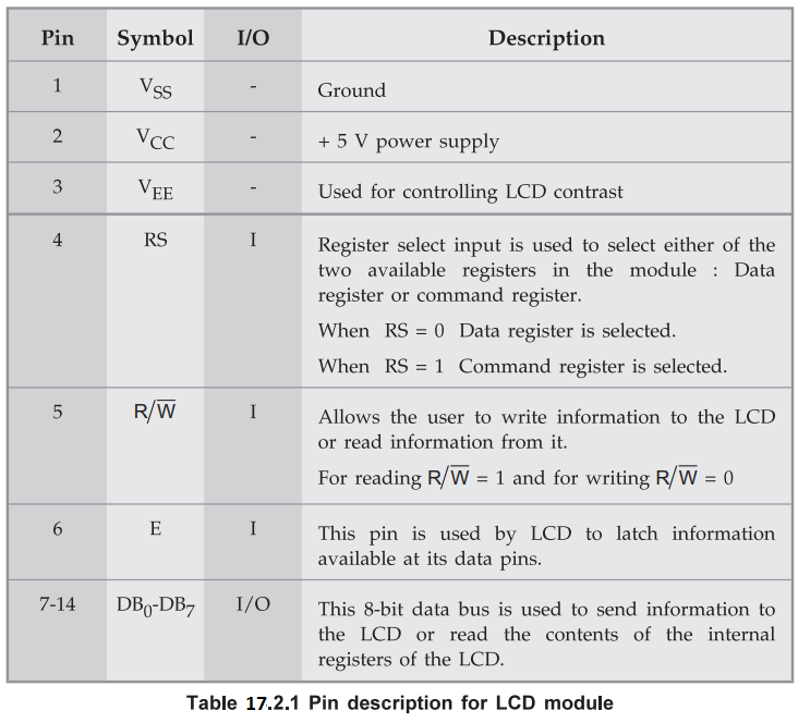
of 20 characters. The module has 14-pins. The function of each pin is given in
the Table 17.2.1.
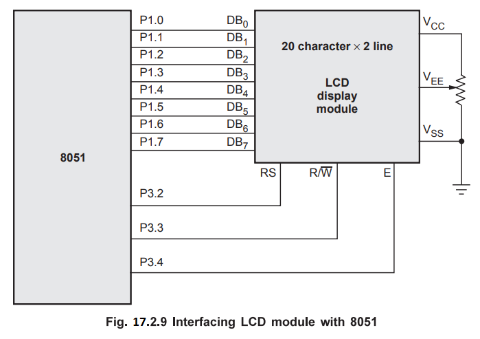
The
Fig. 17.2.9 shows the interfacing of a 20 character × 2 line LCD module with
the 8051. As shown in the Fig. 17.2.9, the data lines are connected to the port
1 of 8051 and control lines RS, ![]() and E are driven by 3.2, 3.3 and 3.4
lines of port 3, respectively. The voltage at VEE pin is adjusted by
a potentiometer to adjust the contrast of the LCD.
and E are driven by 3.2, 3.3 and 3.4
lines of port 3, respectively. The voltage at VEE pin is adjusted by
a potentiometer to adjust the contrast of the LCD.
The
display can be controlled by issuing proper commands to the LCD module. The
Table 17.2.2 lists the command available for LCD module.
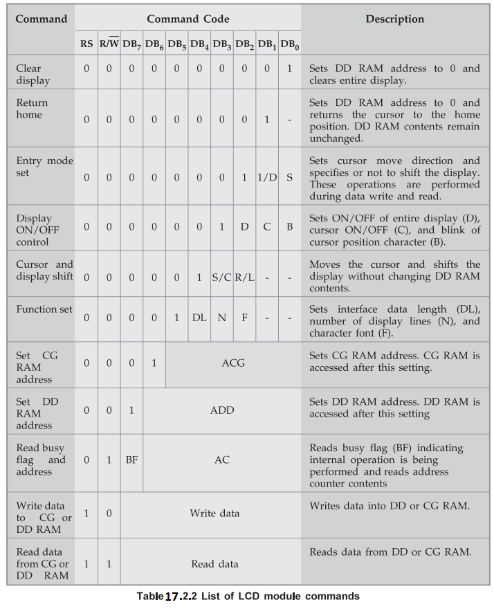
Abbreviations
used in the table
DD
RAM : Display data RAM
CG
RAM : Character generator RAM
ACG
: CG RAM address
ADD
: DD RAM address
AC
: Address counter used for both DD and CG RAM address
1/D
= 1 : Increment 1/D = 0 : Decrement
S
= 1 : Accompanies display shift
S/C
= 1 : Display shift S/C = 0 : Cursor
move
R/L
= 1 : Shift to right R/L = 0 : Shift to left
DL
= 1 : 8-bits DL = 0 : 4-bits
N
= 1 : 2 Lines N = 0 : 1 Line
F
= 1 : 5 × 10 dots F = 0 : 5×7 dots
BF
= 1 Busy in internal operation
BF
= 0 Can accept command or instruction
To
display a message on LCD module, it is
necessary to initialize it by writing series of command codes in the command
register in a proper sequence. The initialization includes command codes for
clearing the display, returning the cursor home, and shifting cursor
automatically after writing a character. After initialisation we can write data
to either DD RAM or CG RAM. Both RAMs are read/write RAMs and have unique
addresses to access each location. To write data in any RAM we have to set the
address for that RAM by issuing proper command. Then we can write data into it
by activating write cycle. To activate write cycle we have to make ![]() signal low, RS signal high, send data on port A and apply high to low pulse of
at least 450 ns of duration on E pin of the module. The DD RAM stores the
characters in their ASCII code whereas CG RAM stores the character in its internally
generated character code. Let us see the 8051 assembly language program to
display 'WELCOME' message on the LCD module. Before sending command or data it
is necessary to check busy flag, i.e. whether LCD is reading or not.
signal low, RS signal high, send data on port A and apply high to low pulse of
at least 450 ns of duration on E pin of the module. The DD RAM stores the
characters in their ASCII code whereas CG RAM stores the character in its internally
generated character code. Let us see the 8051 assembly language program to
display 'WELCOME' message on the LCD module. Before sending command or data it
is necessary to check busy flag, i.e. whether LCD is reading or not.
MAIN
Routine :
MOV
81H,#30H ; Initialise stack pointer
MOV
A,#3CH ; [Send command code to set font = 5×10 dots,
LCALL
COMMAND ; DL = 8-bits and N = 2 lines],
MOV
A,#0EH ; [Send command code to set display
LCALL
COMMAND ; and cursor ON]
MOV
A,#01H ; [Send command code to
LCALL
COMMAND ; clear LCD]
MOV
A,#86H ; [Send command to set DD RAM
LCALL
COMMAND ; address to the seventh location]
MOV
A,#'W'
LCALL
DISPLAY ; Display letter W
MOV
A,#'E'
LCALL
DISPLAY ; Display letter E
MOV
A,#'L'
LCALL
DISPLAY ; Display letter L
MOV
A,#'C’
LCALL
DISPLAY ; Display letter C
MOV
A,#'O'
LCALL
DISPLAY ; Display letter O
MOV
A,#’M'
LCALL
DISPLAY ; Display letter M
MOV
A,#’E'
LCALL
DISPLAY ; Display letter E
SJMP HERE:HERE ; Loop here after displaying
message
COMMAND
Routine :
LCALL
READY ; Check whether LCD is ready ?
MOV
P1, A ; Issue command code
CLR
P3.2 ; Make RS = 0 to issue command
CLR
P3.3 ; Make ![]() = 0 to enable writing
= 0 to enable writing
SETB
P3.4 ; Make E = 1
CLR
P3.4 ; Make E = 0
RET
; Return
READY
Routine :
READ
: CLR P3.4 ; Disable display
CLR
P3.2 ; Make RS = 0 to access command register
MOV
P1,#0FFH ; Configure P1 as an input port
SETB
P3.3 ; Make ![]() = 1 to enable
reading
= 1 to enable
reading
READ
: SETB P3.4 ; Make E = 1
JB
P1.7,READ ; Check DB7 bit. If it is 1, LCD is busy hence check if until it is 0
CLR
P3.4 ; Make E = 0 to disable display
RET
; Return
DISPLAY
Routine :
LCALL
READY ; Check whether LCD is ready ?
MOV
P1, A ; Issue data
SETB
P3.2 ; Make RS = 1 to issue data
CLR
P3.3 ; Make ![]() = 0 to enable
writing
= 0 to enable
writing
SETB
P3.4 ; Make E = 1
CLR
P3.4 ; Make E = 0
RET
; Return
Review Questions
1. Interface a 20 × 2
LCD with 8051 microcontroller and write assembly language program to display
the following message in it at the middle.
HELLO ! ALL
ARE WELCOME
2. Explain the LCD
display interfacing with microcontroller 8051.
3. Explain the
interfacing of keyboard/display with 8051 microcontroller.
4. How to interface a
7 segment display using 8051 microcontroller.
5. Draw the circuit
diagram to interface an LCD display with 8051 microcontroller and explain how to
display a character using LCD display.
6. Explain the
interfacing of four digit 7 segment display to 8051 and its program. AU : Dec.-16, Marks 16
7. Illustrate the
keyboard and display interface with 8051 and write the program to get the input
45H from the external keyboard and display it on the external display device.
8. Design a system
using 8085 or 8051 to blink four LEDs. AU : May-11, 13, 16, 17, Dec.-12,
17, 19
Microprocessors and Microcontrollers: Unit V: (a) Microcontroller Applications : Tag: : - Display Interface