Digital Logic Circuits: Solved Paper
DLC Solved Semester Question Paper 2014 Dec (2013 Reg)
Digital Logic Circuits
Digital Logic Circuits: Solved Paper : Sem – III [EEE] : PART A , B.
Solved Paper
Sem – III [EEE] Regulation 2013
DECEMBER - 2014
Digital Logic Circuits
PART
A - (10 × 2 = 20 Marks)
Note
:
Answer ALL questions.
Q.
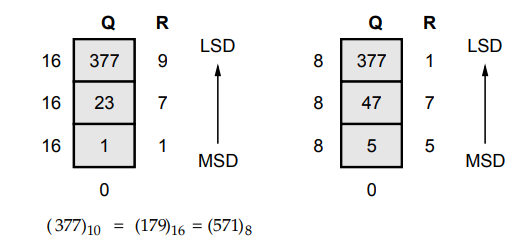
1 Determine (377)10 in octal and hexa-decimal equivalent.
Ans.
:
Q.
2 Compare the totem-pole output with open-collector output.
(Refer
Q.26 of Section 2.10)
Q.
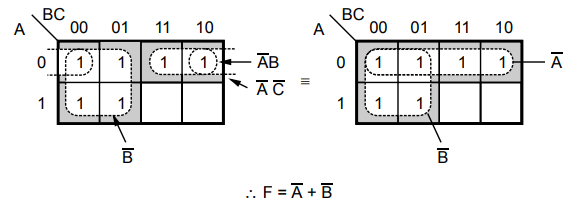
3 Given F = B' + A' B + A' C': Identify the redundant term using K-map.
Ans.
:
The redundant term in given expression is ![]()
Q.
4 Give one application each for multiplexer and decoder.
(Refer
section 3.17.7 and Q.61 of Section 3.20)
Q.
5 Show how the JK flip flop can be modified into a D flip flop or a T
flip-flop. (Refer Q.27 of Section 4.10)
Q.
6 Differentiate between Mealy and Moore models.
(Refer
Q.8 of Section 5.10)
Q.
7 What is a deadlock condition ?
(Refer
Q.15 of Section 5.10)
Q.
8 Draw the block diagram of PLA.
(Refer
Q.9 of Section 9.6)
Q.
9 Write a VHDL code for 2 ×1 MUX.
(Refer
Q.31 of Section 10.22)
Q.
10 State the advantage of package declaration over component declaration.
(Refer
Q.32 of Section 10.22)
PART
B - (5 × 16 = 80 Marks)
Q.11
a) i) Given that a frame with bit sequence 1101011011 is transmitted, it has
been received as 1101011010. Determine the method of detecting the error using
any one error detecting code. (Refer section 1.8.3) [8]
ii)
Draw the MOS logic circuit for NOT gate and explain its operation (Refer
section 2.6.1.1) [8]
OR
b)
i) Explain Hamming code with an example. State its advantages over parity
codes. (Refer section 1.8.3) [8]
ii)
Design a TTL logic circuit for a 3-input NAND gate. (Refer section 2.5.3) [8]
Q.12
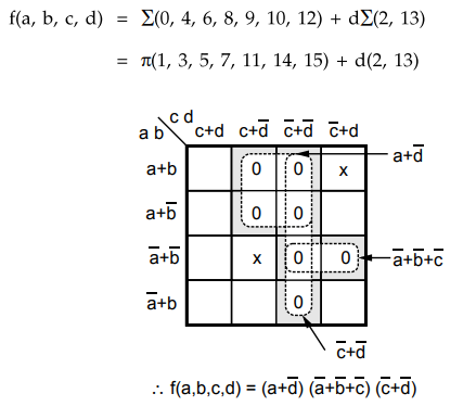
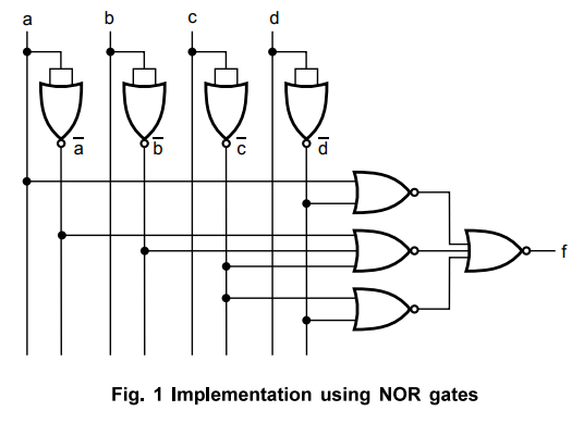
a) i) Minimize the function F(a, b, c, d) = ∑ (0, 4, 6, 8, 9, 10, 12) with d =
∑ (2, 13). Implement the function using only NOR gates. [8]
Ans.
:
f(a,
b, c, d) = ∑ (0, 4, 6, 8, 9, 10, 12) + d ∑ (2, 13)
=
π (1 , 3, 5, 7, 11, 14, 15) + d(2, 13)
We
can implement OR-AND logic by NOR-NOR logic as shown in Fig. 1.
ii)
Design a full subtractor and implement it using logic gates. (Refer section
3.12.2)
OR
b)
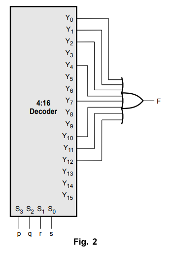
i) Implement the function F(p, q, r, s) = X(0, 1, 2, 4, 7, 10, 11, 12) using
decoder.
Ans.
:
ii)
Design a 4-bit binary to gray code converter and implement it using logic
gates.
(Refer
example 3.21.4) [8]
Q.13
a) i) Design an asynchronous modulo-8 down counter using JK flip-flops. (Refer
section 5.6.1) [8]
ii)
Explain the circuit of a SR flip-flop and explain its operation. (Refer section
4.2) [8]
OR
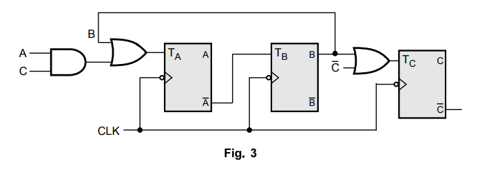
b)
i)Design synchronous sequential circuit that goes through the count sequence 1,
3, 4, 5 repeatedly. Use T flip-flops for your design. [8]
Ans.
:
Step
1 :
Determine the number of flip-flops required.
We
know that 2n ≥ N. Here, N = 5 .’.
n = 3.
Step
2 :
Type of flip-flops to be used : T
Step
3 :
Determine the excitation table for counter.
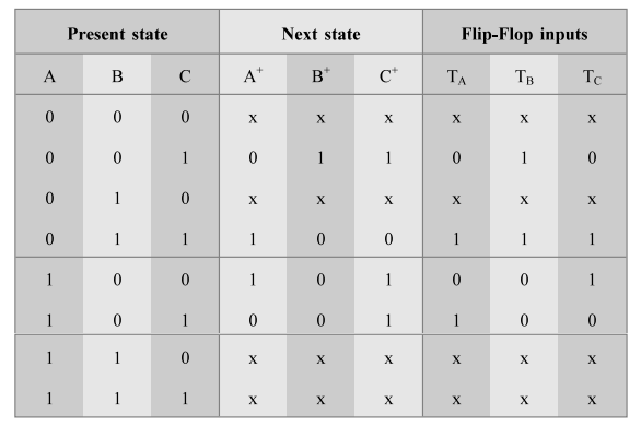
Step
4 :
K-map simplification.
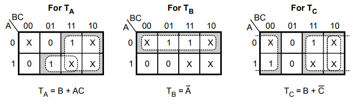
Step 5 : Logic diagram.
ii)
Explain the various types of triggering with suitable diagrams. Compare their
merits and demerits.
(Refer
section 4.1.3) [8]
Q.14
a) Explain the various types of hazards in sequential circuit design and the
methods to eliminate them. Give suitable examples. (Refer section 8.1) [16]
OR
b)
Describe with reasons, the effect of races in asynchronous sequential circuit
design. Explain its types with illustrations. Show the method of race-free
state assignments with examples. (Refer section 7.6.3) [16]
Q.15
a) i)Explain the digital system design flow sequence with the help of a flow
chart. [8]
Ans.
:
In any design process, there are the basic tasks which should be performed in a
sequence. The flow-chart shown in Fig. 4 gives this basic sequence of tasks.
First,
the initial design is generated manually by the designer according to his
views, skills and knowledge. After this, the simulation of the design is
carried out mostly with the help of CAD tools. For the successful simulation,
it is necessary to apply adequate input conditions to the design as well as to
the final product which has to be tested. The simulator checks the designed
product under the original product specifications. This is known that what
should be achieved. So if there are errors, then those are removed and
redesigned product is again simulated. This loop is repeated until the
simulation gives problem-free/error-free product. Once the designed product
performs correctly all of its functions, we call it the 'successful design'.
The
operation of a digital circuit can be verified fastly and accurately using
logic simulation. There are two types of verification techniques, functional
and timing.
The
simulation is referred to as 'functional simulation' when all the functions of
the circuit are verified. After completion of successful functional simulation,
the 'physical design' step is carried out. Physical design includes the
physical location of each chip on the board and the needed wiring pattern. CAD
tools are used for performing this task automatically. After physical design,
the functionality of the circuit is checked. But, eventhough the functional
behaviour is correct, the circuit may operate more slowly than the desired. The
physical wiring on board introduces resistance and capacitance of electrical
signals. The delays are introduced because of logic circuits such as gates.
This reduces the speed of operation of the circuit and thus lead to inadequate
performance. So timing behaviour of the circuit should also be considered. The
simulation which also considers the timing behaviour of the circuit is referred
to as 'timing simulation'.
Thus
in functional simulation, the circuit logical operation is studied by deriving
the truth table of the circuit independent of timing considerations. In timing
simulation, the circuit operation is studied by considering timing behaviour of
the circuit. For example, the waveforms at the output of the gate are observed
when they respond to a given input.

ii)Write
a VHDL code for a 4-bit universal shift register.
(Refer
section 10.16.9)
OR
b)
Explain the concept of behavioural modeling and structural modeling in VHDL.
Take the example of full adder design for both and write the coding. (Refer
sections 10.3.1 and 10.3.3) [16]
Digital Logic Circuits: Solved Paper : Tag: : Digital Logic Circuits - DLC Solved Semester Question Paper 2014 Dec (2013 Reg)
Related Topics
Related Subjects

Digital Logic Circuits
EE3302 3rd Semester EEE Dept | 2021 Regulation | 3rd Semester EEE Dept 2021 Regulation