Digital Logic Circuits: Solved Paper
DLC Solved Semester Question Paper 2015 Dec (2013 Reg)
Digital Logic Circuits
Digital Logic Circuits: Solved Paper : Sem – III [EEE] : PART A, B.
Solved Paper
Sem – III [EEE] Regulation 2013
DECEMBER - 2015
Digital Logic Circuits
Time
: 3 Hours] [Total Marks : 100
PART
A - (10 × 2 = 20 Marks)
Q.1 What is an unit distance code ? Give an example.
(Refer
section 1.7.5)
Q.2
Define Fan-out. (Refer Two Marks Q.3 of Chapter-2)
Q.3
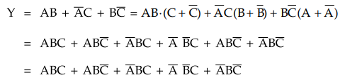
Convert the given expression in canonical SOP form Y = AB + A'C + BC'.
Ans.
:
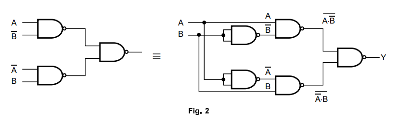
Q.4 Draw the logical diagram of EX-OR gate using
NAND gates.
Ans.
:
The Boolean expression for EX-OR gate is :
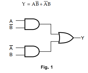
We
can implement AND-OR logic by using NAND-NAND logic as shown in Fig. 2.
Q.5
Draw the truth table and state diagram of SR flip-flop.
(Refer
sections 4.2 and 4.8.2)
Q.6
What is edge triggered flip-flops ?
(Refer
section 4.1.3)
Q.7
What is PROM ?
(Refer
Two Marks Q.10 of Chapter-9)
Q.8
Compare pulsed mode and fundamental mode asynchronous circuit.
(Refer
section 7.2)
Q.9
Write the behavioral model of D flip flop.
(Refer
section 10.14.1)
Q.10
List out the operators present in VHDL.
(Refer
section 10.6.6)
PART
B - (5 × 16 = 80 Marks)
Q.11
a) i) Draw the CMOS logic circuit for NOR gate and explain its operation.
(Refer
section 2.6.5)
ii) Perform the following operation (756)8
- (437) 8 + (725)16.
Express the answer in octal form.
Ans.
:

OR
b)
i) A 12 bit Hamming code word containing 8 bits of data and 4 parity bits is
read from memory. What was the original 8 bit data word that was written into
memory if the 12 bit word read out is as
1)
101110010100 and 2) 111111110100 (Refer example 1.8.12) [12]
ii)
Briefly discuss weighted binary code. (Refer section 1.7.1) [4]
Q.12
a) i) Simplify the boolean function using K-map and implement using only NAND
gates.
F(A,
B, C, D) = ∑ m(0,8,11,12,15) + ∑ d(1,2,4,7,10,14).
Mark
the essential and non-essential prime implicants. [8]
ii)
Design a full subtractor and implement using logic gates. (Refer section
3.12.2) [8]
OR
b)
i) Design a 4 bit BCD to excess 3 code converter and implement using logic
gates.
(Refer
example 3.21.2) [8]
ii)
What is a multiplexer ? Implement the following boolean function with 8 × 1 MUX
and external gates.
F(A,
B, C, D) = ∑m(1,3,4,11,12,13,14,15) [8]
Ans.
:
Refer section 3.17

Q.13
a) i) A sequential circuit with two D flip flops A and B, input X and output Y
is specified by the following next state and output equations
A(t
+ 1) = AX + BX
B(t
+ 1) = A'X
Y
= (A + B)X'
Draw
the logic diagram, derive state table and state diagram .
(Refer
example 5.3.2) [12]
ii)
Realize T flip-flop usig JK flip-flop. (Refer section 4.9.4) [4]
OR
b)
i) Design a synchronous decade counter using T flip flop and construct the
timing diagram. (Refer example 5.9.8) [8]
ii)
Design a Mealy model of sequence detector to detect the pattern 1001.
(Refer
example 5.10.5) [8]
Q.14
a) Design an asynchronous sequential circuit (with detailed steps involved)
that has 2 inputs x1 and x2 and one output z. The circuit
is required to give an output 2 = 1 when x1 = 1, x2 = 1
and x1 = 1 being first.
(Refer
example 7.6.9) [16]
OR
b)
Show how to program the fusible links to get a 4 bit gray code from the binary
inputs using PLA and PAL and compare the design requirements with PROM.
(Refer
example 9.4.4) [16]
Q.
15 a) i) Write a VHDL program for 1 to 4 Demux using dataflow modeling.
Ans
. :
library
ieee;
use
ieee.std_logic_1164.all;
entity
demux4×1 is
port
( din : in std_logic;
sel:
in std_logic_vector (1 downto 0);
dout
: out std_logic_vector (3 downto 0));
end
demux4×1;
architecture
demux4×1_are of demux4×1 is
begin
with
sel select
dout
< = (din & "000") when "00",
('0'
& din & "00") when "01",
("00"
& din & '0') when "10",
("000"
& din) when others;
end
demux4×1_arc;
ii)Write
a VHDL program for full adder using structural modelling.
(Refer
section 10.3.3) [8]
OR
b)
Explain in detail the RTL design procedure.
(Refer
section 10.20)
Digital Logic Circuits: Solved Paper : Tag: : Digital Logic Circuits - DLC Solved Semester Question Paper 2015 Dec (2013 Reg)
Related Topics
Related Subjects

Digital Logic Circuits
EE3302 3rd Semester EEE Dept | 2021 Regulation | 3rd Semester EEE Dept 2021 Regulation