Digital Logic Circuits: Solved Paper
DLC Solved Semester Question Paper 2015 May (2013 Reg)
Digital Logic Circuits
Digital Logic Circuits: Solved Paper : Sem – III [EEE] : PART A, B.
Solved Paper
Sem – III [EEE] Regulation 2013
MAY - 2015
Digital Logic Circuits
Time
: 3 Hours] [Total Marks : 100
PART
A - (10 x 2 = 20 Marks)
Q.1
Convert:
a)
(475.25)s to its decimal equivalent.
(Refer
section 1.2.3)
b)
(549.B4)16 to its binary equivalent.
(Refer
example 1.3.4)
Q.2
Define propagation delay.
(Refer
Two Marks Q.5 of Chapter-2)
Q.3
Convert the given expression in cannonical SOP form Y = AC + AB + BC. (Refer
example 3.2.1)
Q.4
Simplify the expression
(Refer example 3.1.2)
Q.5
Convert T Flip Flop to D flip-flop.
(Refer
Section 4.9.7)
Q.6
State the rules for state assignment.
(Refer
Section 5.4.2)
Q.7
State the difference between static 0 and static 1 hazard.
(Refer Two Marks
Q.4 of Chapter-8)
Q.8
What is PROM ?
(Refer
Two Marks Q.10 of Chapter-9)
Q.9
What is a package in VHDL ?
(Refer
Section 10.2.4)
Q.10 Write the behavioral modeling code for a D
flip flop.
(Refer Section 10.14.1)
PART
B - (5 × 16 = 80 Marks)
Q.11
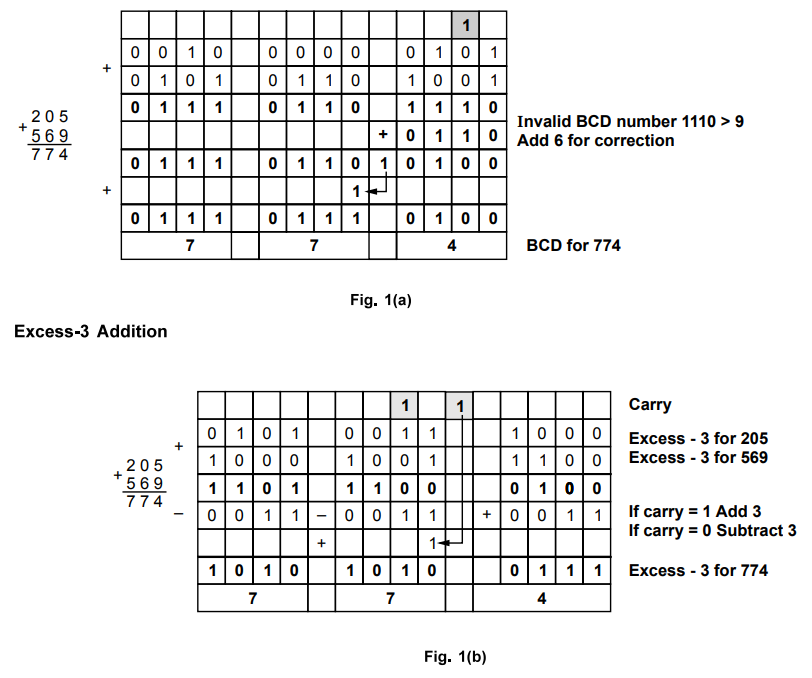
a) i) Perform the following addition using BCD and excess-3 addition (205+569).
Ans.
:
BCD Addition
ii)Encode
the binary word 1011 into seven bit even parity Hamming code.
(Refer
example 1.8.4)
OR
b)
i) With circuit schematic, explain the operation of a two input TTL NAND gate
with totem-pole output.
(Refer
section 2.5.2)
ii)
Compare totem pole and open collector outputs. (Refer section 2.5.6)
Q.12
a) i) Reduce the following function using K-map
F(A,B,C,D)
= πM(0,2,3,8,9,12,13,15) (Refer example 3.5.3)
ii)
Design a full adder using two half-adders and an OR gates.
(Refer
section 3.11.2)
OR
b)
i) Design a BCD to excess 3 code converter.
(Refer
example 3.21.2)
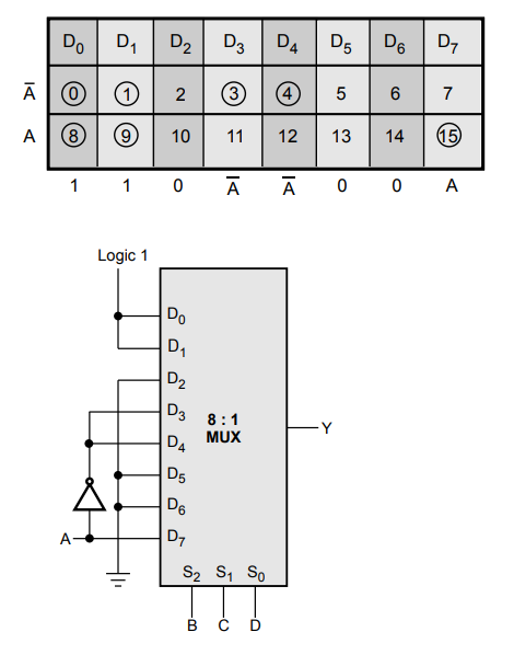
ii)
Implement the following boolean function using 8:1 MUX : F(A,B,C,D) = ∑m(0,1,3,4,8,9,15)
;
Ans.
:
Q.13
a) i) Explain the operation of a master slave JK flip flop.
(Refer
section 4.5)
ii)
Design a 3-bit bidirectional shift register.
(Refer
section 6.3.5)
OR
b)
i) Design a MOD-5 synchronous counter using JK flip-flops.
(Refer
example 5.9.1)
ii)
Design a sequence detector to detect the sequence 101 using JK flip flop.
(Refer
section 5.10)
Q.14
a) Design an asynchronous sequential circuit that has two inputs X2
and 1 and one output Z. When X1 = 0, the output Z is 0.
The first change in X2 that occurs while X1 is 1 will
cause output Z to be 1. The output Z will remain 1 until X1 returns
to 0. (Refer example 7.6.5)
b)
i)Implement the following function using PLA:
F(x,y,z)
= ∑ m(1,2,4,6)
OR
ii) For the given boolean function, obtain the hazard-free circuit F(A,B,C,D) = ∑m(1,3,6,7,13,15)
Ans.
:

Q.15
a) i) Write a VHDL code to realize a full adder using.
i)
Behavioral modeling (Refer section 10.3.1)
ii)
Structural modeling (Refer section 10.3.3) [16]
OR
b)
Write the VHDL code to realize a 3-bit gray code counter using case statement. [16]
Ans.
:
library
ieee;
use
ieee.std_logic_1164.all;
entity
GCT is
port
(elk, Reset: in std_logic;
Q
: buffer std_logic_vector ( 2 downto 0));
end
GCT;
architecture
counter_3b of GCT is
begin
counter
: process (clk)
variable
temp : std_logic.vector (2 downto 0) : = "000";
begin
if
rising_edge (clk) then
if
Reset = '0' then
case
temp is
when
"000" = > temp : = “001”
when
"001" = > temp : = “011”
when
"010" = > temp : = "110";
when
"011" => temp : = "010";
when
"100" => temp : = "000";
when
"101" => temp : = "100";
when
"110" => temp : = "111";
when
"111" = > temp : =
"101";
when
other = > temp : = "000";
end
case;
else
temp
: = "000";
end
if; end if;
Q
< = temp;
end
process counter;
end
counter_3b;
Digital Logic Circuits: Solved Paper : Tag: : Digital Logic Circuits - DLC Solved Semester Question Paper 2015 May (2013 Reg)
Related Topics
Related Subjects

Digital Logic Circuits
EE3302 3rd Semester EEE Dept | 2021 Regulation | 3rd Semester EEE Dept 2021 Regulation