Digital Logic Circuits: Solved Paper
DLC Solved Semester Question Paper 2016 May (2013 Reg)
Digital Logic Circuits
Digital Logic Circuits: Solved Paper : Sem – III : PART A, B.
Solved Paper
Sem – III [EEE] Regulation 2013
MAY - 2016
Digital Logic Circuits
Time
: 3 Hours]
[Total
Marks : 100
PART
A - (10 × 2 = 20 Marks)
Q.1
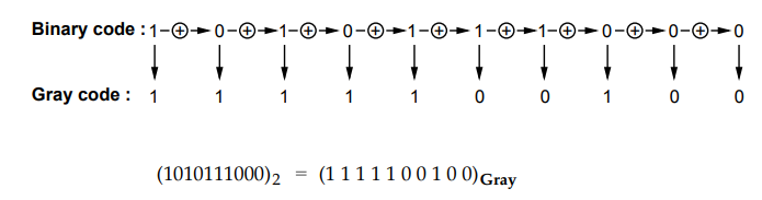
Convert the following binary code into a Gray Code :
10101110002
Ans.
:
Q.2
Define fan-in and fan-out.
(Refer
Two Marks Q.4 of Chapter - 2)
Q.3
Write the POS representation of the following SOP function :
f(x,
y, z) = ∑ m (0, 1, 3, 5, 7)
Ans.
:
f(x,
y, z) = ∑ m (0, 1, 3, 5, 7)
=
πM(2, 4, 6)
Q.4
Design a half subtractor.
(Refer
section 3.12.1)
Q.5
Give the characteristic equation and characteristic table of SR flip-flop.
(Refer
Fig. 4.2.2)
Q.6
State any two differences between Moore and Mealy state machines.
(Refer
section 5.2.3)
Q.7
What are the two types of asynchronous sequential circuits ?
(Refer
Two Marks Q.3 of Chapter 7)
Q.8
State the difference between PROM, PLA and PAL.
(Refer table 9.5.1)
Q.9
What is dataflow modelling in VHDL? Give its basic mechanism.
(Refer
section 10.3.2)
Q.10 Write the VHDL code to realize a 2 x 1
multiplexer. (Refer example 10.7.4)
PART
B - (5 × 16 = 80 Marks)
Q.11
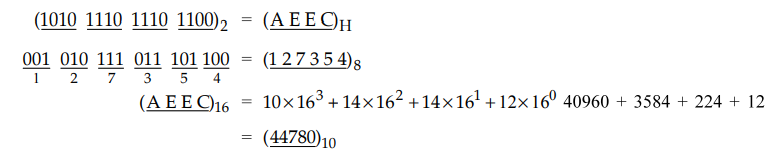
a) i) Convert 10101110111011002 into its octal, decimal and
hexadecimal equivalent. [6]
Ans.
:
ii)
Deduce the odd parity hamming code for the data : 1010. Introduce an error in the
LSB of the hamming code and deduce the steps to detect the error.
(Refer
example 1.8.8) [10]
OR
b)
i) With circuit schematic explain the operation of a two input TTL NAND gate.
(Refer
section 2.5.2) [8]
ft)
With circuit schematic and explain the operation and characteristics of a ECL
gate.
(Refer
section 2.7) [8]
Q.12
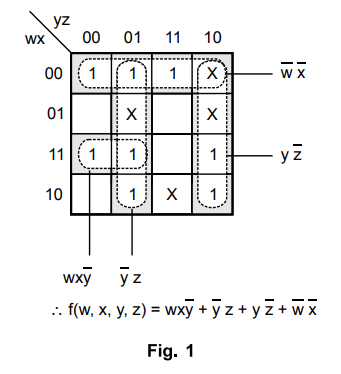
a) i) Simplify the following function using Karnaugh map.
f(w,
x, y, z) = ∑m(0, 2, 3, 9, 20, 22, 23, 24) + ∑d(2, 5, 6, 11) [8]
Ans.
:
ii)
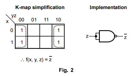
Implement the following function using only NAND gates :
fix,
y, z) = E ∑ (0, 2, 4, 6)
Ans.
:
OR
i)
Design a BCD to excess-3 code converter.
(Refer
example 3.21.2)
ii)
Design a full adder and implement in using suitable multiplexer.
(Refer
section 3.11.2 and example 3.17.13)
Q.
13 a) i) Explain the operation of a JK master slave flip flop.
(Refer
section 4.5)
ii)
Design a MOD-5 counter using T flip flops.
(Refer
similar example 5.9.2)
OR
b)
i) Design a serial adder using Mealy state model.
(Refer
section 5.4.7)
ii)
Explain the state minimization using partitioning procedure with a suitable
example.
(Refer
section 5.4.1.2)
Q.
14 a) i) What are static - 0 and static - 1 hazards? Explain the removal of
hazards using hazard covers in K-map.
(Refer
section 8.1)
ii) Explain cycles and races in asynchronous
sequential circuits.
(Refer
section 7.6.2)
OR
b)
i) What are transition table and flow table? Give suitable examples.
(Refer
section 7.6)
ii)
Implement the following function using PLA and PAL :
f(x,
y, z) = ∑ m (0, 1, 3, 5, 7)
(Refer
similar examples 9.3.8 and 9.4.3)
Q.
15 a) i) Explain the various operators supported by VHDL.
(Refer
section 10.6.6)
ii)
Write the VHDL code to realize a decade counter with behavioural modelling.
(Refer
similar example in section 10.15.6)
OR
b)
i) Explain functions and subprograms with suitable examples.
(Refer
sections 10.10 and 10.13)
ii)
Write the VHDL code to realize a 4 - bit parallel binary adder with structural
modelling and write the test bench to verify its functionality.
(Refer
sections 10.9 and 10.21) [10]
Digital Logic Circuits: Solved Paper : Tag: : Digital Logic Circuits - DLC Solved Semester Question Paper 2016 May (2013 Reg)
Related Topics
Related Subjects

Digital Logic Circuits
EE3302 3rd Semester EEE Dept | 2021 Regulation | 3rd Semester EEE Dept 2021 Regulation