Digital Logic Circuits: Solved Paper
DLC Solved Semester Question Paper 2017 Dec (2013 Reg)
Digital Logic Circuits
Digital Logic Circuits: Solved Paper : Sem – III [EEE] : PART - A, B, C.
DECEMBER - 2017
Digital Logic Circuits
Solved Paper
Sem - III [EEE] Regulation 2013
Time
: 3 Hours] [Total Marks : 100
PART
- A (10 × 2 = 20 Marks)
Q.1
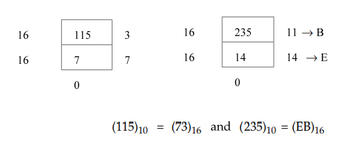
Convert (115)10 and. (235) 10
to hexadecimal numbers.
Ans.
:
Q.2
What is a gray code and mention its advantages ?
(Refer
section 1.7.5)
Q.3
What is a K-map ?
(Refer
section 3.3)
Q.4
Compare decoder and demultiplexer.
(Refer
Two Marks Q.60 of chapter-3)
Q.5
What do you mean by race around condition in a flip flop ?
(Refer
Two Marks Q.12 of chapter-4)
Q.6 What is a presettable counter and ripple
counter 1
(Refer
Two Marks Q.21 of chapter-5)
Q.7
What happens to the information stored in a memory location after it has been
read and write operation ?
Ans.
:
After read operation the information stored in the memory location remains
unchanged. After write operation the information stored in the memory location
is overwritten.
Q.8
What is Programmable Logic Array ? (Refer Two Marks Q.3 of chapter-9)
Q.9
Define modularity.
Ans.
:
Modularity is the degree to which a system's components may be separated and
recombined.
Q.10
What are the languages that are combined together to get VHDL language ?
Ans.
:
Sequential language, concurrent language, net- list language, tuning
specification and waveform generation language are combined together to get
VHDL language.
PART
- B (5 × 13 = 65 Marks)
Q.11
a) Explain in detail about error detecting and error correcting code.
(Refer
section 1.8) [13]
OR
b)
Write short notes on following : [13]
i)
RTL ii) DTL iii) TTL and iv) ECL
(Refer
sections 2.3, 2.4, 2.5 and 2.7)
Q.12
a) i) Plot the logical expression 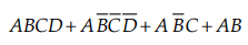 on a 4 - variable K - map;
obtain the simplified expression from the maps. [7]
on a 4 - variable K - map;
obtain the simplified expression from the maps. [7]
Ans.
:
OR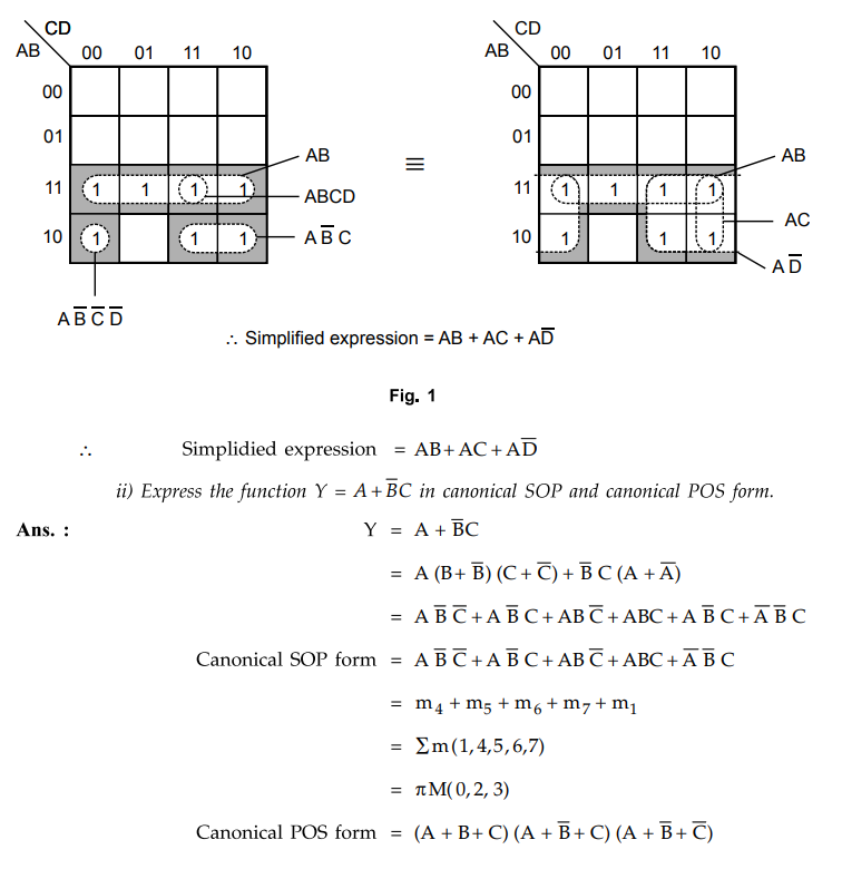
b)
Design a 4 - bit gray code to binary converter and express using logic gates.
Ans.
:
Table 1 shows the truth table for gray code to binary code converter.
Q.13
a) Explain the operation, state diagram and characteristics of T - flip - flop
and master - slave JKflip - flop.
(Refer
sections 4.6 and 4.5) [13]
OR
b)
Explain in detail about different shift registers. (Refer section 6.3) [13]
Q.14
a) Discuss about the hazards in asynchronous sequential circuit and the ways to
eliminate them.
(Refer
section 7.6.3) [13]
OR
b)
i) Write short notes on PLA and PAL. (Refer sections 9.3 and 9.4) [7]
ii)
What is hazards ? Explain hazards in digital circuits. (Refer section 8.1) [6]
Q.15
a) Write a VHDL code to realize a full adder using behavioural modeling and
structural modeling.
(Refer
listing 10.3.1 and 10.9.4) [10]
OR
b)
i) Discuss briefly the packages in VHDL. (Refer sections 10.2.4 and 10.2.5) [6]
ii)
Write an VHDL coding for realization of clocked SR flip - flop. (Refer listing
10.14.1) [7]
PART
- C (1 × 15 = 15 Marks)
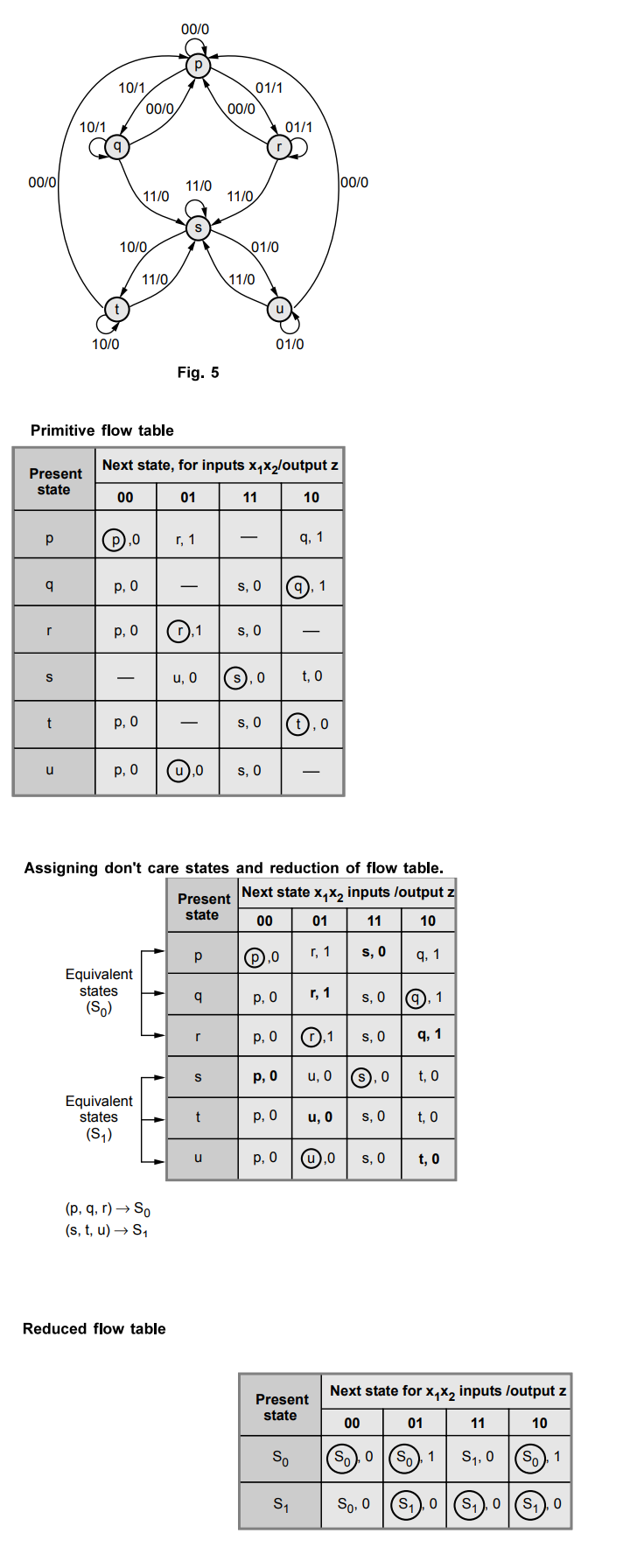
Q.16
a) Design an asynchronous sequential circuit with two inputs x1 and
x2 and one output Z. Initially, both inputs are equal to zero. When
x1 or x2 becomes 1, the output Z becomes 1. When the
second input also becomes 1, the output changes to 0. The output stays at 0
until the circuit goes back to the initial state. [15]
Ans.
: State diagram

b)
i) Design a full adder using 4×1 multiplexer, also write its truth table and
draw the logical diagram.
(Refer
example 3.17.14)
ii)
Describe level triggering and edge triggering.
(Refer
section 4.1.3)
Digital Logic Circuits: Solved Paper : Tag: : Digital Logic Circuits - DLC Solved Semester Question Paper 2017 Dec (2013 Reg)
Related Topics
Related Subjects

Digital Logic Circuits
EE3302 3rd Semester EEE Dept | 2021 Regulation | 3rd Semester EEE Dept 2021 Regulation