Digital Logic Circuits: Solved Paper
DLC Solved Semester Question Paper 2017 May (2013 Reg)
Digital Logic Circuits
Digital Logic Circuits: Solved Paper : Sem – III [EEE] : PART - A, B, C
Solved Paper
Sem – III [EEE] Regulation 2013
MAY - 2017
Digital Logic Circuits
Time
: 3 Hours] [Total Marks : 100
PART
- A (10 × 2 = 20 Marks)
Q.1
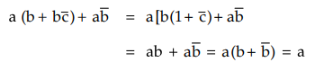
Reduce a(b + bc) + ab'.
Ans.
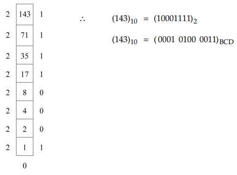
Q. 2 Convert 14310 into its Unary and Unary coded decimal equivalent.
Ans.
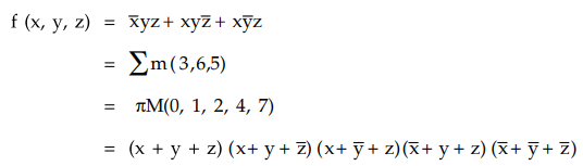
Q.3
Write the POS form of the SOP expression f (x, y,z) = x 'yz + xyz + xy 'z.
Ans.
:
Q.4
Design a Half Subtractor.
(Refer
section 3.12.1)
Q.5
Give the characteristic equation and characteristic table of a T Flip Flop.
(Refer
section 4.6)
Q.6
State the differences between Moore and Melay state machines.
(Refer
section 5.2.3)
Q.7
What is a flow table ? Give example.
(Refer
section 7.6.1)
Q.8
State the difference between PROM, PAL and PLA.
(Refer
section 9.5)
Q.9
Give the syntax for package declaration and package body in VHDL.
(Refer
sections 10.2.4 and 10.2.5)
Q.10
Write the VHDL code for 2x1 multiplexer using behavioral modeling.
(Refer
example 10.7.3)
PART
- B (5 × 13 = 65 Marks)
Q.11
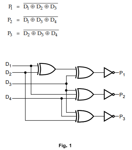
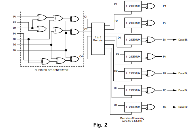
a) i) Design a odd - parity hamming code generator and detector for 4 - bit
data and explain their logic.
Ans.
:
For
P1 : D1, D2 and D3 bits are
considered
For
P2 : D1, D3 and D4 bits are
considered
For
P3 : D2, D3 and D4 bits are
considered
Ex
- OR logic gives logic 1 output for odd number ones in the inputs.
We
need to set priority bit = 0 if there are odd number of ones in the input
Therefore,
for odd parity
In
the decoder circuit, code word is applied as input. Then check bits are
generated by the checker bit generator to check the parity bits. These check
bits locates the error in the code word by means of decoder circuit. The output
of decoder enables a demultiplexer which are connected to the input code words.
If no error occurs then the select line of demultiplexer flows the input form
line 10 and the II is set to logic T'. So from the logic OR gate we can obtain
the data. Now if an error occur then the select line of the demultiplexer flows
the code word from line II and 10 is set to logic 'O'. Thus inverting the bits,
the error bit is corrected and thus we can obtain the error free data. A
decoder circuit of hamming code for 4 bit data word is also shown in Fig. 2
ii)
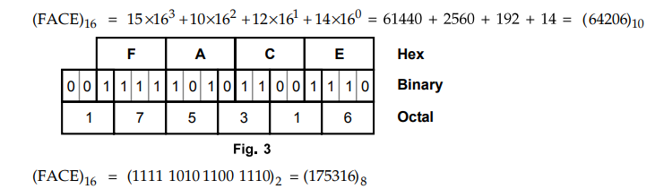
Convert FACE16 into its binary, octal and decimal equivalent.
Ans
. :
OR
b)
i) With circuit schematic explain the working of a two - input TTL NAND gate.
(Refer
section 2.5.2)
ii)
Compare totem pole and open collector outputs.
(Refer
section 2.5.6)
Q.12
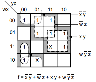
a) i) Reduce the following minterms using Karnaugh – Map
f
(w, x, y, z) = ∑ m (0,1,3,5,6,7,8,12,14) + ∑ d (9,15)
Ans.
ii)
Implement the following function using a suitable multiplexer
f
(a,b,c) = ∑ m(3,7,4,5) (Refer similar example 3.17.7)
OR
b)
i) Design a 3 × 8 decoder and explain its operation as a minterm generator.
(Refer
example 3.19.1)
ii)
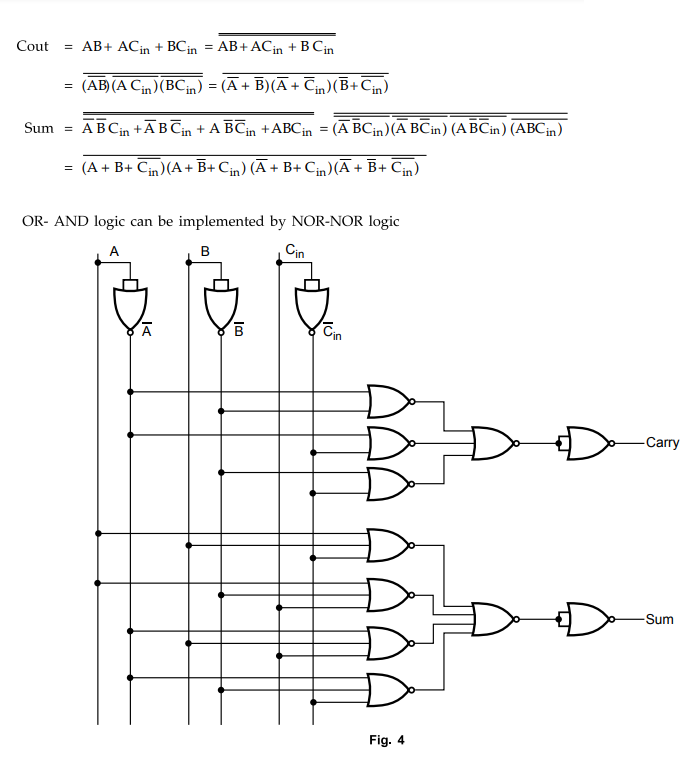
Design a full adder using only NOR gates.
Ans.
:
Refer Table 3.11.2 and Fig. 3.11.6.
We
have,
Q.13
a) i) Draw and explain the operation of a Master - Slave JK Flip Flop.
(Refer
section 4.5)
ii)
Design a 5 - bit ring counter and mention its applications.
(Refer
section 6.6)
OR
b)
i) Design a 4 - bit parallel - in serial - out shift register using D Flip
Flops.
(Refer
section 6.3.3) [7]
ii)
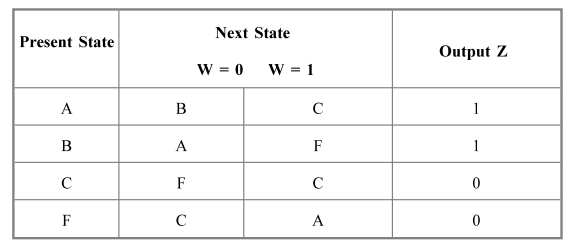
Using partitioning minimization procedure reduce the following state table :
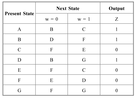
Ans.
:
Refer section 5.4.1.2 for procedure
Step
1 : 1 – equivalent
P1
= (A, B, D)(C, E, F, G)
Step
2 : 2 – equivalent
P2
= (A, B, D)(C, E, G) (F)
Step
3 : 3 – equivalent
P3
= (A, D)(B)(C, E, G)(F)
The
states in the common blocks of P3 are equivalent and redundant.
Therefore, states A = D and C = E = G.
Minimized
state table :
Q.14
a) A control mechanism for a vending machine accepts nickels and dimes. It
despense merchandise when 20 cents is deposited; it does not give change if 25
cents is deposited. Design the FSM that implements the required control, using
as few states as possible. Find a suitable assignment and derive next - state
and output expressions. [13]
Ans.
:
Coins are deposited one at a time. The coin-sensing mechanism generates signals
N = 1 and D = 1 when it sees a nickel or a dime, respectively. It is impossible
to have N = D = 1 at the same time. Following the insertion of a coin for which
the sum equals or exceeds 20 cents, the machine releases the merchandise and
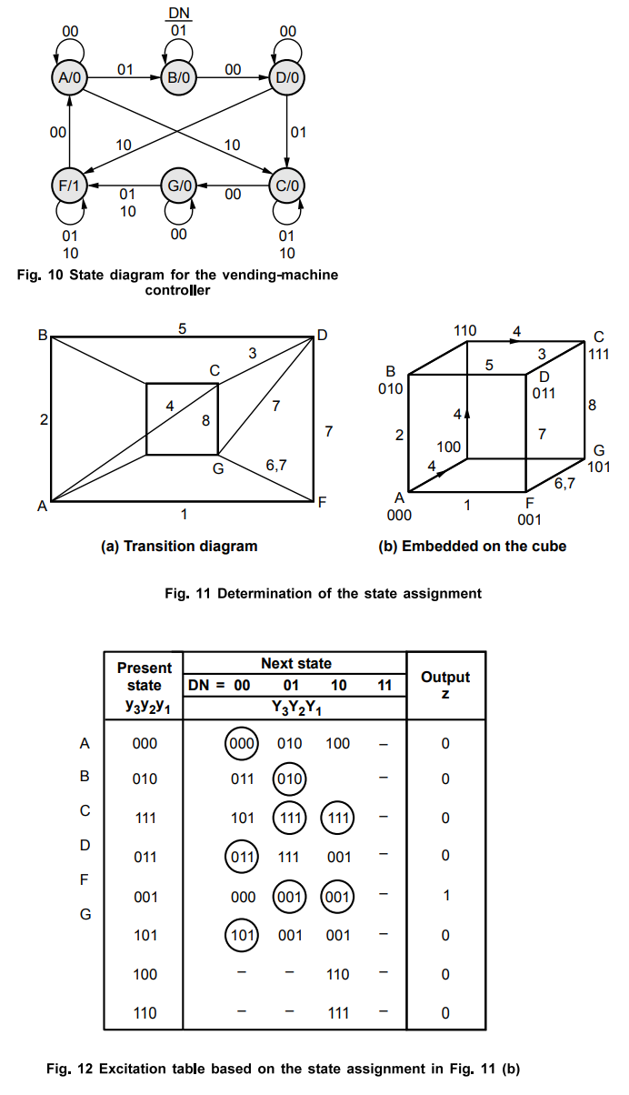
resets to the initial state.
Fig.
5 shows a state diagram for the required FSM. It is derived using a straight
forward approach in which all possible sequences of depositing nickels and
dimes are enumerated in a treelike structure. To keep the diagram uncluttered,
the labels D and N denote the input conditions DN = 10 and DN = 01,
respectively. The condition
DN
= 00 is labeled simply as 0. The merchandise is released in states F, H, and K,
which are reached after 20 cents has been deposited, and in states I and L,
upon a deposit of 25 cents.
The
corresponding flow table is given in Figure 2. It can be reduced using the
partitioning procedure as follows
P1
= (ADGJ)(BE)(C)(FIL)(HK)
P2
= (A)(D)(GJ)(B)(E)(C)(FIL)(HK)
P3
= P2
Using
G to represent the equivalent states G and J , F to represent F, I , and L, and
H to represent H and K yields a partially reduced flow table in Fig. 7. The
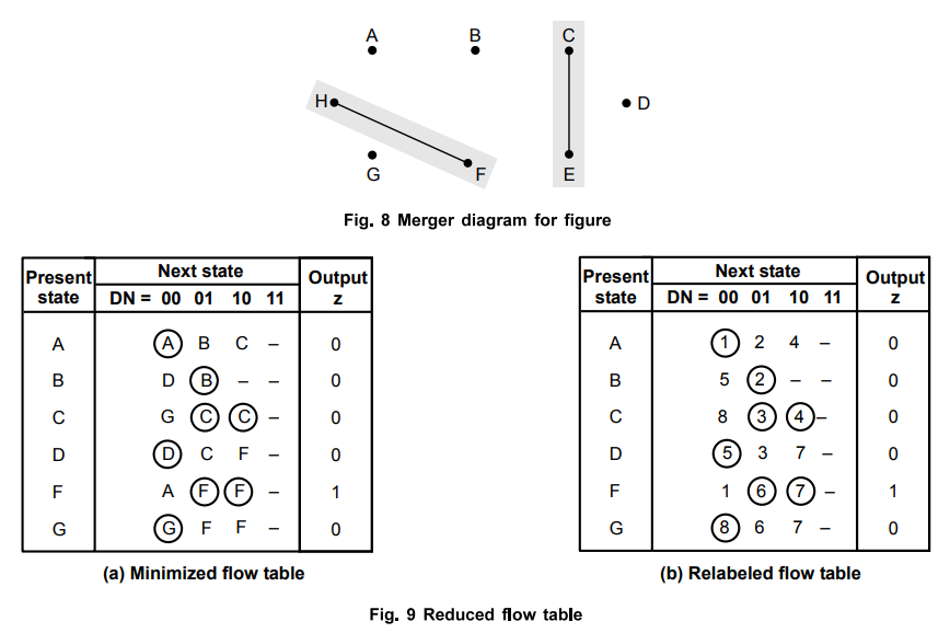
merger diagram for this table is presented in Figure 4. It indicates that
states C and E can be merged, as well as F and H. Thus the reduced flow table
is obtained as shown in Fig. 9(a). The same information is depicted in the form
of a state diagram in Fig. 10.
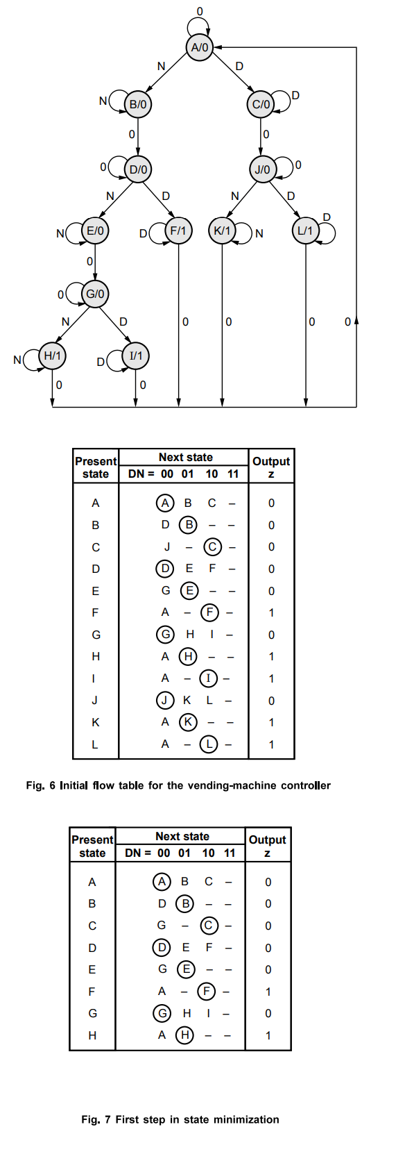
Next
a suitable state assignment must be found. The flow table is relabeled in Fig.
9(b) to associate a unique number with each stable state. Then the transition
diagram in Fig. 11(a) is obtained. Since we wish to try to embed the diagram
onto a three dimensional cube, eight vertices are shown in the figure. The
diagram shows two diagonal transitions. The transition between D and G (label
7) does not matter, because it is only an alternative path. The transition from
A to C (label 4) is required, and it can be realized via unused states as
indicated in Fig. 11(b). Therefore, the transition diagram can be embedded onto
a three-dimensional cube as shown. Using the state assignment from this figure,
the excitation table in Fig. 12 is derived.
OR
b)
i) Implement the following logic and analyse for the pressure of any hazard 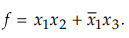 .
If hazard is present briefly explain the type of hazard and design a hazard -
free circuit. (Refer section 8.1.1) [7]
.
If hazard is present briefly explain the type of hazard and design a hazard -
free circuit. (Refer section 8.1.1) [7]
ii)
Implement the following functions using programmable logic array :
f1
( x, y, z) = ∑ m(1,3,5,7)
f2(x,y,z)
= ∑ m(2,4,6) (Refer similar example 9.3.3)
Q.15
a) Design a 3 - bit magnitude comparator and write the VHDL code to realize it
using structural modeling.
(Refer
listing 10.9.8) [13]
b)
Design a 4 × 4 array multiplier and write the VHDL code to realize it using
structural modeling. [13]
Ans.
:
VHDL Code for 4×4 Array Multiplier
entity
Array_Mult is
port
(X. Y : in bit_vector (3 downto 0);
P
: out bit_vector (7 downto 0);
end
Anray_Mult;
architecture
Behavioral of Array_Mult is
signal
Cl, C2, C3; bitvector (3 downto 0);
signal
SI, S2, S3; bit_vector (3 downto 0);
signal
XY1, XY2, XY3; bit_vector (3 downto 0);
component
FullAdder
port
(X, Y, Cin : in bit;
Cout,
Sum : out bit);
end
component;
component
HalfAdder
port
(X, Y : in bit;
Cout,
Sum : out bit);
end
component;
begin
XYO(O)
← X(0) and Y(0); XY1(O) ← X(0) and Y(l);
XYO(l)
← X(l) and Y(0); XY1(1) ← X(1) and Y(l);
XY0(2)
← X(2) and Y(0); XY1(2) ← X(2) and Y(l);
XY0(3)
← X(3) and Y(0); XY1(3) ← X(3) and Y(l);
XY2(0)
← X(0) and Y(2); XY3(0) ← X(0) and Y(3);
XY2(1)
← X(l) and Y(2); XY3(1) ← X(1) and Y(3);
XY2(2)
← X(2) and Y(2); XY3(2) ← X(2) and Y(3);
XY2(3)
← X(3) and Y(2); XY3(3) ← X(3) and Y(3);
FA1
: FullAdder port map (XY0(2), XY1(1), Cl(0), Cl(l), Sl(l));
FA2
: FullAdder port map (XY0(3), XY1(2), Cl(l), Cl(2), Sl(2));
FA3
: FullAdder port map (Sl(2), XY2(1), C2(0), C2(l), S2(l));
FA4
: FullAdder port map (Sl(3), XY2(2), C2(l), C2(2), S2(2));
FA5
: FullAdder port map (Cl(3), XY2(3), C2(2), C2(3), S2(3));
FA6
: FullAdder port map (S2(2), XY3(1), C3(0), C3(l), S3(l));
FA7
: FullAdder port map (S2(3), XY3(2), C3(l), C3(2), S3(2));
FA8
: FullAdder port map (C2(3), XY3(3), C3(2), C3(3), S3(3));
HA1
: HalfAdder port map (XYO(l), XY1(O), C1(O), Sl(0));
HA2
: HalfAdder port map (XY1(3), Cl(2), Cl(3), Sl(3));
HA3
: HalfAdder port map (Sl(l), XY2(0), C2(0), S2{0));
HA4
: HalfAdder port map (S2(l), XY3(0), C3(0), S3(0));
P(0)
← XY0(0); P(l) ← Sl(0); P(2) ← S2(0);
P(3)
← S3(0); P(4) ← S3(l); P(5) ← S3(2);
P(6)
← S3(3); P(7) ← C3(3);
end
Behavioral;
PART
C (1 × 15 = 15 Marks)
Q.
16 a) Design a CMOS inverter and explain its operation. Comment on its
characteristics such as Fan - in, Fan - out power dissipation, propagation
delay and noise margin. Compare its advantages over other logic families.
(Refer
sections 2.6.3, 2.2 and 2.6.7) [15]
OR
b)
Write the VHDL code for the given state diagram, using behavioral modeling.
Design it using one - hot state assignment and implement it using Programmable
Array Logic (PAL). [15]
 Ans.
:
VHDL code for given state diagram
Ans.
:
VHDL code for given state diagram
LIBRARY
IEEE:
USE
IEEE.std_logic_1164.all;
ENTITY
SEQ IS,
PORT
(Clock, Reset, W : IN STDLOGIC;
Z
: OUT_STD LOGIC);
End
SEQ;
ARCHITECTURE
Behaviour of SEQ IS,
TYPE
state_type IS (A, B, C);
SIGNALY
: state_type;
BEGIN
IF
Reset = '0' THEN
Y
= A;
ELSEIF
(clock1 EVENT AND CLOCK = T') THEN
CASE
Y IS
WHEN
A ⇒
if
W = '0' THEN
Y<
= A;
ELSE
Y
< = B;
END
IF;
WHEN
B ⇒
IF
W = '0' THEN
Y
< A;
ELSE
Y
< = C;
END
IF;
WHEN
C ⇒
IFW
'0'THEN
Y
< = A;
ELSE
Y
< = C;
END
IF;
END
CASE;
END
IF;
END
PROCESS;
Z
< = '1' WHEN Y = C ELSE '0';
END
BEHAVIOR
State
table for the given sequential circuit is shown in table 1
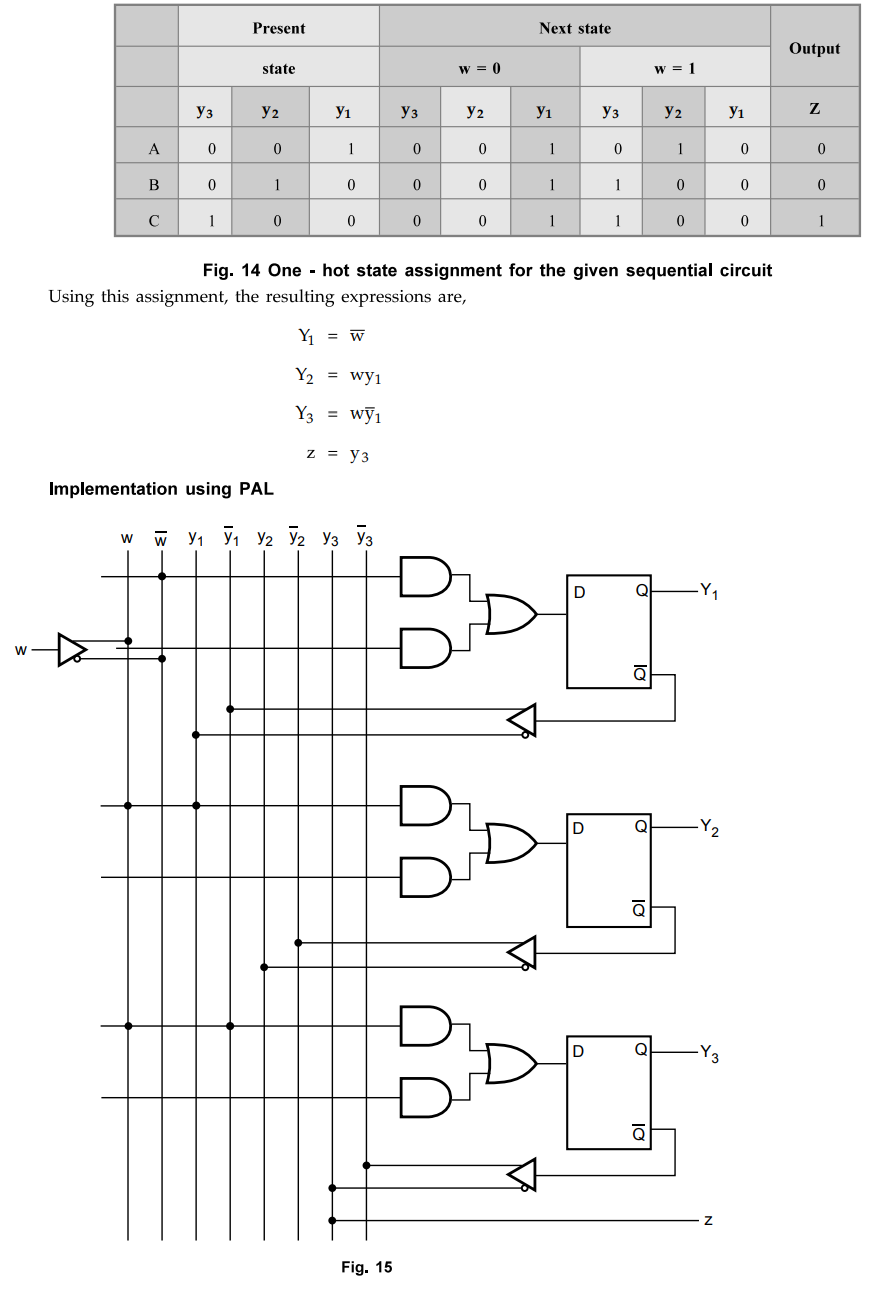
Fig.
14 shows how one-hot state assignment can be applied to the given sequential
circuit. Because there are three states, it is necessary to use three state
variables. The chosen assignment is to represent the states A, B, and C using
the valuations y3 y2 yi = 001, 010, and 100, respectively. The remaining five
valuations of the state variables are not used. They can be treated as don't
cares in the derivation of the next-state and output expressions.
Digital Logic Circuits: Solved Paper : Tag: : Digital Logic Circuits - DLC Solved Semester Question Paper 2017 May (2013 Reg)
Related Topics
Related Subjects

Digital Logic Circuits
EE3302 3rd Semester EEE Dept | 2021 Regulation | 3rd Semester EEE Dept 2021 Regulation