Digital Logic Circuits: Solved Paper
DLC Solved Semester Question Paper 2018 Dec (2017 Reg)
Digital Logic Circuits
Digital Logic Circuits: Solved Paper : Sem - III [EEE] : PART A , B, C
Solved Paper
Sem - III [EEE] Regulation 2017
DECEMBER - 2018
Digital Logic Circuits
Time
: 3 Hours] [Maximum Marks 100
Note
: Answer ALL questions.
PART
A - (10 × 2 = 20 Marks)
Q.
1 Draw the DTL based NAND gate.
(Refer
section 2.4)
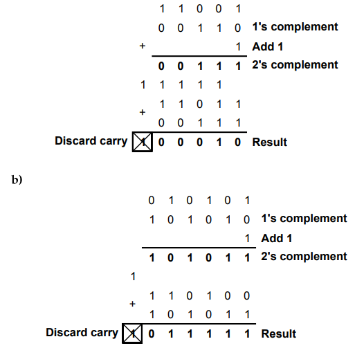
Q.
2 Perform subtraction on the following unsigned binary numbers using the
2's-complement of the subtrahend
(a) 11011 - 11001 (b) 110100 - 10101.
Ans.
: a)
Q.3
Mention the dependency of output in combinational circuits.
(Refer
section 3.10)
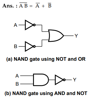
Q.
4 Draw the NAND gate circuit using NOT, AND and OR gates.
Ans
. :
Q.5.
Write the role of master clock generator in synchronous circuits.
Ans.
:
In synchronous circuits, the synchronization is achieved by a timing device
called a master clock generator.
Q.6
Comment about a presettable counter and ripple counter.
(Refer
Q.21 of Chapter - 5)
Q.7
Draw the block diagram of asynchronous sequential circuit.
(Refer
section 7.2)
Q.8
Outline about PLA. (Refer section 9.3)
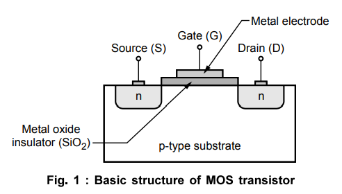
Q.9
Draw the basic structure of MOS transistor.
Ans.
:
Q.10
List the language that are combined together to get VHDL language.
(Refer
Q.10 of Dec.-17)
PART
B - (5 × 13 = 65 Marks)
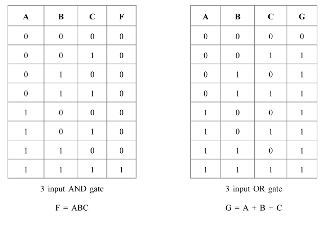
Q.
11 a) Assume a 3 - input AND gate with output F and a 3-input OR gate with G
output. Show the signals of the outputs F and G as functions of the three
inputs ABC. Use all 8 possible combinations of inputs ABC. [13]
Ans
. :
b)
Show that a positive logic NAND gate is a negative long NOR gate and vice
versa.
Ans.
:

Q.12
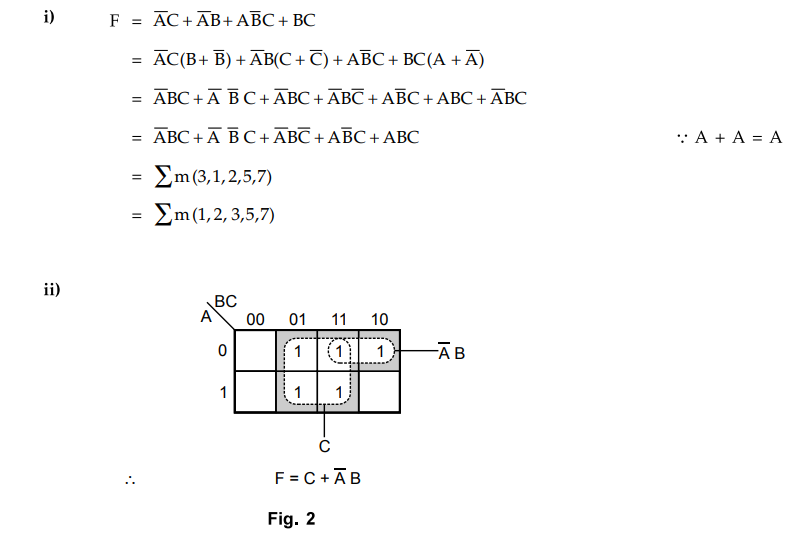
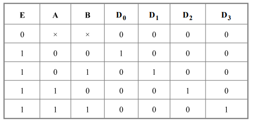
a) Given the following Boolean function F = A C + A B + ABC
i)
Express it in sum of minterms.
ii)
Find the minimal sum of products expression.
Ans.
:
OR
b)
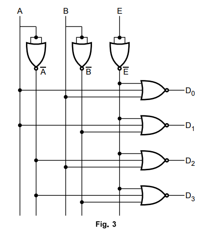
Draw the logic diagram of a 2-to-4 line decoder using NOR gates only. Include
an enable input.
Ans. :
Step
2 :
Deriving Expressions for output
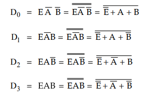
Step
3 :
Logic Diagram
Q.13
a) Explain the operation state diagram and characteristics of a T flip-flop and
master slave JK flip-flop.
(Refer
section 4.6)
OR
b)
Describe the design procedure with neat diagram about 4 bit bidirectional shift
register with parallel load.
(Refer
sections 4.5 and 4.6)
Q.14
a) Discuss the operation of SR Latch with NOR and NAND gates analysis.
(Refer
section 4.1.4) [13]
OR
b)
Illustrate about hazards in sequential circuits and the steps to avoid hazards
in it.
(Refer
section 8.1.2) [13]
Q.15
a) Explain the structure and working principles of TTL based Totem-pole output
configuration.
(Refer
section 2.5.4) [13]
OR
b)
Write a VHDL code to realize a half adder using behavioral modeling and
structural modeling.
(Refer
section 10.7.1 and Refer listing 10.9.2) [13]
PART
C - (1 × 15 = 15 Marks)
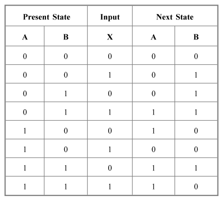
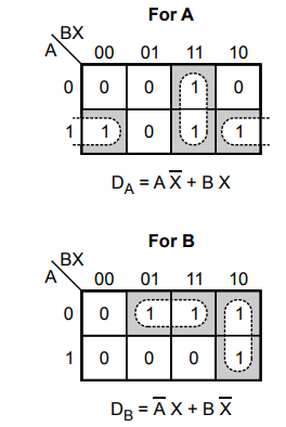
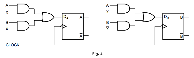
Q.16
a) Design a sequential circuit with two D flip-flops A and B and one input x
when x = 0 the state of the circuit remains the same. When x = 1, the circuit
goes through the state transitions from 00 to 01 to 11 to 10 back to 00 and
repeats. [15]
Ans.
: State Table :
K-map
simplification for A :
Logic
Diagram :
OR
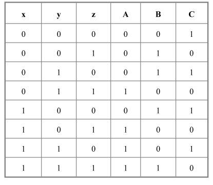
b)
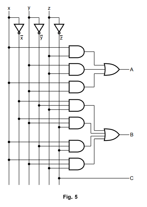
Design a combinational circuit with three inputs, x, y and z and the three
outputs. A, B and C when the binary input is 0, 1, 2 or 3 the binary output is
one greater than the input. When the binary input is 4, 5, 6 or 7, the binary
output is one less than the input. [15]
Ans.
: Truth Table :
K-map
simplification for A :
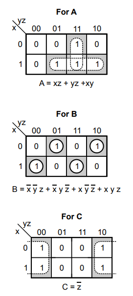
Logic
Diagram :
Digital Logic Circuits: Solved Paper : Tag: : Digital Logic Circuits - DLC Solved Semester Question Paper 2018 Dec (2017 Reg)
Related Topics
Related Subjects

Digital Logic Circuits
EE3302 3rd Semester EEE Dept | 2021 Regulation | 3rd Semester EEE Dept 2021 Regulation