Electron Devices and Circuits: Unit IV: Multistage and Differential Amplifiers
Emitter Coupled Differential Amplifier
Equivalent circuit, Mode Operation
• The transistorised differential amplifier basically uses the emitter biased circuits which are identical in characteristics.
Emitter Coupled Differential Amplifier
AU
: Dec.-12, 17,18, May-16
•
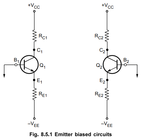
The transistorised differential amplifier basically uses the emitter biased
circuits which are identical in characteristics. Such two identical emitter
biased circuits are shown in the Fig. 8.5.1.
•
The two transistors Q1 and Q2 have exactly matched
characteristics. The two collector resistances. RC1 and RC2
are equal while the two emitter resistances RE1 and RE2
are also equal.
Thus
RC1 = RC2
and
RE1 = RE2
•
The magnitudes of + Vcc and -VEE are also same. The differential amplifier can
be obtained by using such two emitter biased circuits. This is achieved by
connecting emitter E1 of Q1 to the emitter E2 of Q2.
Due to this, REI appears in parallel with RE2 and the combination can be
replaced by a single resistance denoted as Rg. The base B1 of Q1 is
connected to the input 1 which is VS1 while the base B2 of
Q2 is connected to the input 2 which is VS2 . The supply
voltages are measured with respect to ground. The balanced output is taken
between the collector C1 of Q1 and the collector C2
of Q2. Such an amplifier is called emitter coupled differential
amplifier. The two collector resistances are same hence can be denoted as Rc.
The complete circuit diagram of such a basic dual input, balanced output
differential amplifier is shown in the Fig. 8.5.2.
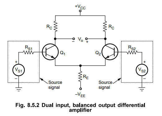
•
As the output is taken between two output terminals, none of them is grounded,
it is called balanced output differential amplifier.
•
Let us study the circuit operation in the two modes namely
i)
Differential mode operation
ii)
Common mode operation.
1. Differential Mode Operation
•
In the differential mode, the two input signals are different from each other.
Consider the two input signals which are same in magnitude but 180° out of
phase. These signals, with opposite phase can be obtained from the center tap
transformer. The circuit used in differential mode operation is shown in the
Fig. 8.5.3.
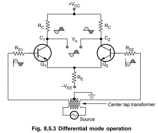
• Assume that the sine wave on the base of Q1 is positive going while on the base of Q2 is negative going. With a positive going signal on the base of Q1 an amplified negative going signal develops on the collector of Q1 Due to positive going signal, current through RE also increases and hence a positive going wave is developed across RĚ. Due to negative going signal on the base of Q2, an amplified positive going signal develops on the collector of Q2. And a negative going signal develops across RE, because of emitter follower action of Q2.
•
So signal voltages across RĚ, due to the effect of Q1 and
Q2 are equal in magnitude and 180° out of phase, due to matched pair
of transistors. Hence these two signals cancel each other and there is no
signal across the emitter resistance. Hence there is no a.c. signal current
flowing through the emitter resistance. Hence RE in this case does not
introduce negative feedback.
•
While Vo is the output taken across collector of Q1 and collector
of Q2. The two outputs on collector 1 and 2 are equal in magnitude
but opposite in polarity. And VQ is the difference between these two signals,
e.g. +10 - (-10) = + 20. Hence the difference output Vo is twice as
large as the signal voltage from either collector to ground.
2. Common Mode Operation
•
In this mode, the signals applied to the base of Q1 and Q2
are derived from the same source. So the two signals are equal in magnitude as
well as in phase. The circuit diagram is shown in the Fig. 8.5.4.
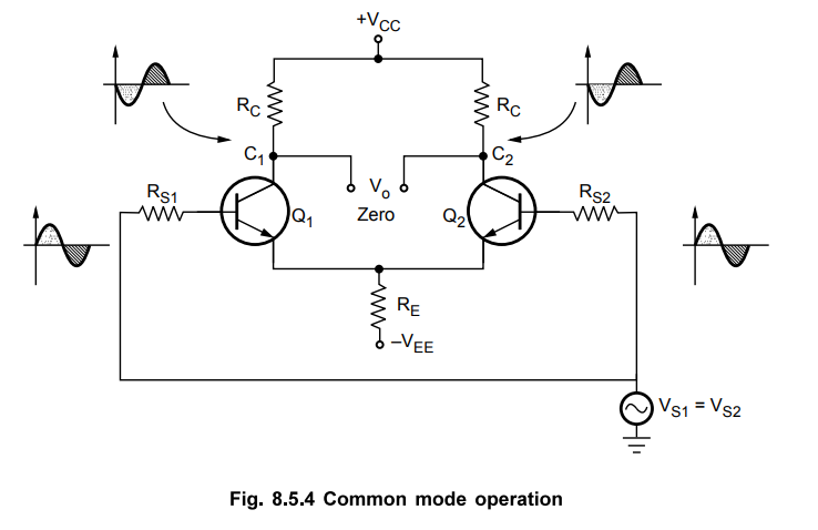
•
In phase signal voltages at the bases of Q1 and Q2 causes
in phase signal voltages to appear across RE, which add together. Hence RE
carries a signal current and provides a negative feedback. This feedback
reduces the common mode gain of differential amplifier.
• While the two signals causes in phase
signal voltages of equal magnitude to appear across the two collectors of Q1
and Q2. Now the output voltage is the difference between the two
collector voltages, which are equal and also same in phase, e.g. (10) - (10) = 0.
Thus the difference output Vo is almost zero, negligibly small.
Ideally it should be zero.
Review Questions
1. Draw the circuit of emitter coupled differential amplifier
and explain its operation in differential mode and common mode.
2. Explain the working of a differential amplifier.
AU : Dec.-17, Marks 8
3. Explain the working of a single ended input differential
amplifier.
Electron Devices and Circuits: Unit IV: Multistage and Differential Amplifiers : Tag: : Equivalent circuit, Mode Operation - Emitter Coupled Differential Amplifier
Related Topics
Related Subjects

Electron Devices and Circuits
EC3301 3rd Semester EEE Dept | 2021 Regulation | 3rd Semester EEE Dept 2021 Regulation