Linear Integrated Circuits: Unit II: Characteristics of Op-amp
Equivalent Circuit of Practical Op-amp
Characteristics, Circuit Diagram, Solved Example Problems
The circuit which represents op-amp parameters in terms of physical components, for the analysis purpose is called equivalent circuit of an op-amp. The equivalent circuit of an op-amp is shown in the Fig. 2.11.1.
Equivalent Circuit of Practical Op-amp
The
circuit which represents op-amp parameters in terms of physical components, for
the analysis purpose is called equivalent circuit of an op-amp. The equivalent
circuit of an op-amp is shown in the Fig. 2.11.1.

The
circuit shows the op-amp parameters like input resistance, output resistance,
the open loop voltage gain in terms of circuit components like Rin,
Ro etc. The op-amp amplifies the difference between the two input
voltages.
Vo
= AOLVd = AOL(V1 - V2)
where
AOL = Large signal open loop voltage gain.
Vd
= Difference voltage V1 - V2.
V1
= Noninverting input voltage with respect to ground.
V2
= Inverting input voltage with respect to ground.
Ri
= Input resistance of op-amp.
Ro
= Output resistance of op-amp.
The
output voltage is directly proportional to the difference voltage Vd.
It
is to be noted that the op-amp amplifies difference voltage and not the
individual input voltages. Thus the output polarity gets decided by the
polarity of the difference voltage Vd.
The
voltage source AOLVd is the Thevenin's equivalent voltage
source while Ro is the Thevenin's equivalent resistance looking back into the
output terminals.
The
equivalent circuit plays an important role in analysing various op-amp
applications as well as in studying the effects of feedback on the performance
of op-amp.
1. Practical Op-amp Characteristics
The
characteristics of an ideal op-amp can be approximated closely enough, for many
practical op-amps. But basically the practical op-amp characteristics are
little bit different than the ideal op-amp characteristics.
The
various characteristics of a practical op-amp can be described as below.
a)
Open loop gain : It is the voltage gain of the op-amp
when no feedback is applied. Practically it is several thousands.
b)
Input impedance : It is finite and typically greater than
1 MQ. But using FETs for the input stage, it can be increased upto several
hundred MQ.
c)
Output impedance : It is typically few hundred ohms. With
the help of negative feedback, it can be reduced to a very small value like 1
or 2 ohms.
d)
Bandwidth : The bandwidth of practical op-amp in
open loop configuration is very small. By application of negative feedback, it
can be increased to a desired value.
e)
Input offset voltage : Whenever both the input terminals
of the op-amp are grounded, ideally, the output voltage should be zero.
However, in this condition, the practical op-amp shows a small non zero output
voltage. To make this output voltage zero, a small voltage in millivolts is
required to be applied to one of the input terminals. Such a voltage makes the
output exactly zero. This d.c. voltage, which makes the output voltage zero,
when the other terminal is grounded is called input offset voltage denoted as
Vios. How much voltage, to which terminal and with what polarity, to be
applied, is specified by the manufacturer in the datasheet. The input offset
voltage depends on the temperature. The concept of input offset voltage is
shown in the Fig. 2.11.2.

The
Vios can be positive or negative hence absolute value of the Vios
is mentioned in the data sheet.
The
smaller the value of Vios , better is the matching of the input terminals.
The
input offset voltage depends on the temperature.
Many
time voltage to one of the input terminals is applied with the proper polarity
so as to null the output, keeping other input terminal grounded. For ideal
op-amp, Vios is zero, hence practical op-amp model is generally shown as in the
Fig. 2.11.3 with the indication of the input offset voltage. For op-amp 741 C
the input offset voltage is 6 mV.

f)
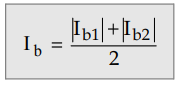
Input bias current : The average value of the two currents
flowing into the op-amp input terminals is called input bias current and
denoted as Ib. It is shown in the Fig. 2.11.4.
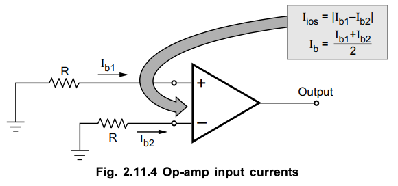
Mathematically
it is expressed as,
g) Input offset current : It is seen that the input stage of the op-amp is the dual input differential amplifier and the input terminals are the base terminals of the two transistors as shown in the Fig. 2.11.5. Hence the input currents of op-amp are the base currents of the two transistors Q1 and Q2 used in the input stage. Ideally, Q1 and Q2 must be perfectly matched and two base currents must be equal. But practically the two input base currents differ by small amount.
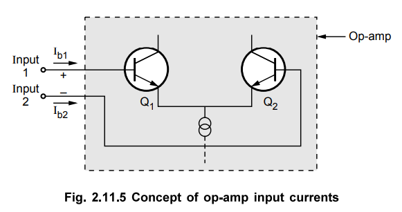
The
algebraic difference between the currents flowing into the two input terminals
of the op-amp is called input offset current and denoted as Iios
Mathematically
it is expressed as,
Iios
= | Ib1 - Ib2|
Where
Ib1 = Current entering into noninverting input terminal
and
Ib2 = Current entering into inverting input terminal
Ideally
Iios is zero while for op-amp 741C, maximum value of Iios
is 200 nA.
This
current is responsible to produce the output though input terminals are
grounded.
Example
2.11.1 If the base currents for the emitter coupled transistors
of a differential amplifier are 18 μA and 22 μA, determine
i)
Input bias current ii) Input offset
current for an op-amp.
Solution:
The two input base currents are, Ibl = 18 μA and Ib2 = 22
μA
i)
The input bias current is
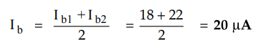
ii) The input offset current is
Iios
= |Ib1 - Ib2| = |18 – 22| = 4µA
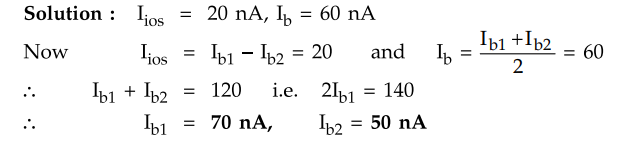
Example
2.11.2 For a particular op-amp, the input offset current is 20 nA while input
bias current is 60 nA. Calculate the values of two input bias currents.
Solution
:
Review Questions
1. Draw and explain practical op-amp equivalent circuit.
2. Explain the practical characteristics of op-amp.
3. Define the following for a practical op-amp : i) Input offset
voltage ii) Input offset current iii) Input bias current.
Linear Integrated Circuits: Unit II: Characteristics of Op-amp : Tag: : Characteristics, Circuit Diagram, Solved Example Problems - Equivalent Circuit of Practical Op-amp
Related Topics
Related Subjects

Linear Integrated Circuits
EE3402 Lic Operational Amplifiers 4th Semester EEE Dept | 2021 Regulation | 4th Semester EEE Dept 2021 Regulation